-
How to Increase Charging Current While Shrinking Overall Solution Size for Portable Electronics
How to Increase Charging Current While Shrinking Overall Solution Size for Portable Electronics
Alvaro Aguilar
Modern portable electronic devices include a high-capacity lithium-ion battery to power the features we know and love, such as high-definition cameras, edge-to-edge high-resolution touchscreens and a high-speed data connection. As the list of features continues to increase, so does the battery capacity required to support them, along with the charge current required to recharge the battery in a reasonable amount of time.
One key consideration for system designers is balancing battery capacity, charging time and device temperature while charging. This last element is important, not only to enhance the user experience but to improve battery safety and lifetime. Given a battery’s capacity, you can reduce the charging time by increasing the charging current, while controlling the equipment temperature by reducing the total power loss inside the device.
Switch-mode battery-charger efficiency typically drops at higher current levels, which translates to a larger power loss and higher equipment temperatures. A buck-based battery charger can typically achieve higher efficiency by sacrificing solution size; for example, a larger inductor with a lower resistance might increase the efficiency of a typical design at high currents.
TI’s latest companion battery charger, the bq25910, is based on a three-level buck converter technology, which gives you the flexibility to increase efficiency by 5 percentage points while shrinking the solution size by 2x. This is an exceptional improvement in efficiency and solution size, and translates to a 50% increase in charge current for a fixed loss budget when compared to the older generation chargers.
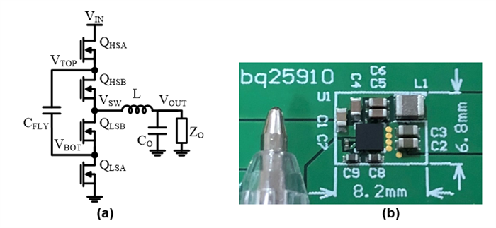
The three-level buck converter illustrated in Figure 1 is a combination of a switched capacitor and switched inductor circuit with no fundamental duty-cycle limitation. With the addition of a flying capacitor, CFLY, balanced at VIN/2, the circuit reduces voltage stress on switching MOSFETs by half, doubles the effective switching frequency at VSW and reduces the volt-seconds across the inductor by half. The gate-driving scheme is similar to that of a two-phase buck converter. A complementary signal drives the outer FETs, QHSA and QLSA, with duty cycle D = VOUT/VIN. A second complementary signal of equal duty cycle drives the inner FETs, QHSB and QLSB, but is phase-shifted by 180 degrees.
 Figure 1 The Three-level Buck Converter Circuit Used in the bq25910 (a); the Device’s Total Solution Size Is 56mm2, Including All Power Components (b)
Assuming that CFLY remains balanced at VIN/2, the VSW node can be presented with three different voltages: VIN, VIN/2 and GND. The reduced voltage across the inductor dictates the ripple current in the circuit, which is a key parameter in selecting the required inductance. Because the inductor is typically the largest physical component of a switching converter, reducing its requirements translates to significant savings in solution size. This makes new applications possible such as height constrained, high charge current designs. Moreover, a smaller inductance will actually yield lower losses, hence the higher overall efficiency.
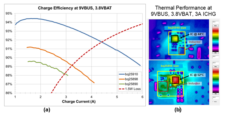
The addition of a flying capacitor allows the three-level buck converter to reduce switching losses in semiconductor devices as well as the size and loss of the external inductor, dramatically increasing efficiency. Even a small efficiency improvement can translate into a higher charge current, as explored by my colleague Fernando Lopez Dominguez in his blog post. By improving efficiency by 5 percentage points, the bq25910 offers an increase in charge current from 2.9A to 4.35A for an equal power loss of 1.5W, all while reducing the total solution size 2x. You can see this illustrated in Figure 2, which compares the efficiency, size and temperature of the bq25910 to previous-generation chargers.
 Figure 2 The bq25910 Has +5% Higher Efficiency and +50% Higher Current for Fixed Losses (a); and Runs 8°C Cooler at Half the Size (b)
With each new generation, our portable electronic devices are becoming more feature-rich. These new features require both a larger battery capacity and a larger physical area to provide an enhanced user experience. This, in turn, places stringent requirements on battery chargers: they must occupy less space and charge a larger battery in an equal or shorter timeframe. The fact that buck converter-based chargers typically trade off efficiency for size requires a new technology that can provide both.
The bq25910 offers considerable improvements in fast and cool battery charging, all while reducing solution size. Consider taking advantage of this innovative solution in your next battery charger design with high current and high efficiency requirements. Order a bq25910 evaluation module today to enhance your next design with this truly innovative solution.
Additional Resources
- Watch a video explaining the 3-level buck converter.
- Explore TI’s portfolio of products that can charge your battery faster, cooler and safer.
- Check out these two training videos to help jumpstart your next project on long taper time and issues why your battery may not be charging.
IMPORTANT NOTICE AND DISCLAIMER
TI PROVIDES TECHNICAL AND RELIABILITY DATA (INCLUDING DATASHEETS), DESIGN RESOURCES (INCLUDING REFERENCE DESIGNS), APPLICATION OR OTHER DESIGN ADVICE, WEB TOOLS, SAFETY INFORMATION, AND OTHER RESOURCES “AS IS” AND WITH ALL FAULTS, AND DISCLAIMS ALL WARRANTIES, EXPRESS AND IMPLIED, INCLUDING WITHOUT LIMITATION ANY IMPLIED WARRANTIES OF MERCHANTABILITY, FITNESS FOR A PARTICULAR PURPOSE OR NON-INFRINGEMENT OF THIRD PARTY INTELLECTUAL PROPERTY RIGHTS.
These resources are intended for skilled developers designing with TI products. You are solely responsible for (1) selecting the appropriate TI products for your application, (2) designing, validating and testing your application, and (3) ensuring your application meets applicable standards, and any other safety, security, or other requirements. These resources are subject to change without notice. TI grants you permission to use these resources only for development of an application that uses the TI products described in the resource. Other reproduction and display of these resources is prohibited. No license is granted to any other TI intellectual property right or to any third party intellectual property right. TI disclaims responsibility for, and you will fully indemnify TI and its representatives against, any claims, damages, costs, losses, and liabilities arising out of your use of these resources.
TI’s products are provided subject to TI’s Terms of Sale (www.ti.com/legal/termsofsale.html) or other applicable terms available either on ti.com or provided in conjunction with such TI products. TI’s provision of these resources does not expand or otherwise alter TI’s applicable warranties or warranty disclaimers for TI products.
Mailing Address: Texas Instruments, Post Office Box 655303, Dallas, Texas 75265
Copyright © 2023, Texas Instruments Incorporated