LM5106 100-V Half-Bridge Gate Driver With Programmable Dead-Time
1 Features
- Drives Both a High-Side and Low-Side N-Channel MOSFET
- 1.8-A Peak Output Sink Current
- 1.2-A Peak Output Source Current
- Bootstrap Supply Voltage Range up to 118-V DC
- Single TTL Compatible Input
- Programmable Turnon Delays (Dead-Time)
- Enable Input Pin
- Fast Turnoff Propagation Delays (32 ns Typical)
- Drives 1000 pF With 15-ns Rise and 10-ns Fall Time
- Supply Rail Undervoltage Lockout
- Low Power Consumption
- 10-Pin WSON Package (4 mm × 4 mm) and 10-Pin VSSOP Package
2 Applications
- Solid-State Motor Drives
- Half-Bridge and Full-Bridge Power Converters
- Two Switch Forward Power Converters
3 Description
The LM5106 is a high-voltage gate driver designed to drive both the high-side and low-side N-channel MOSFETs in a synchronous buck or half-bridge configuration. The floating high-side driver can work with rail voltages up to 100 V. The single control input is compatible with TTL signal levels and a single external resistor programs the switching transition dead-time through tightly matched turnon delay circuits. The robust level shift technology operates at high speed while consuming low power and provides clean output transitions. Undervoltage lockout (UVLO) disables the gate driver when either the low side or the bootstrapped high-side supply voltage is below the operating threshold. The LM5106 is offered in the 10-pin VSSOP or the thermally enhanced 10-pin WSON plastic package.
Device Information(1)
| PART NUMBER | PACKAGE | BODY SIZE (NOM) |
|---|---|---|
| LM5106 | VSSOP (10) | 3.00 mm × 3.00 mm |
| WSON (10) | 4.00 mm × 4.00 mm |
- For all available packages, see the orderable addendum at the end of the datasheet.
Simplified Block Diagram

4 Revision History
Changes from C Revision (March 2013) to D Revision
- Added Pin Configuration and Functions section, ESD Ratings table, Feature Description section, Device Functional Modes, Application and Implementation section, Power Supply Recommendations section, Layout section, Device and Documentation Support section, and Mechanical, Packaging, and Orderable Information section Go
Changes from B Revision (March 2013) to C Revision
- Changed layout of National Data Sheet to TI formatGo
5 Pin Configuration and Functions

Pin Functions
| PIN | DESCRIPTION | APPLICATION INFORMATION | |
|---|---|---|---|
| NO. | NAME | ||
| 1 | VDD | Positive gate drive supply | Decouple VDD to VSS using a low ESR/ESL capacitor, placed as close to the IC as possible. |
| 2 | HB | High-side gate driver bootstrap rail | Connect the positive terminal of bootstrap capacitor to the HB pin and connect negative terminal to HS. The Bootstrap capacitor should be placed as close to IC as possible. |
| 3 | HO | High-side gate driver output | Connect to the gate of high-side N-MOS device through a short, low inductance path. |
| 4 | HS | High-side MOSFET source connection | Connect to the negative terminal of the bootststrap capacitor and to the source of the high-side N-MOS device. |
| 5 | NC | Not connected | |
| 6 | RDT | Dead-time programming pin | A resistor from RDT to VSS programs the turnon delay of both the high- and low-side MOSFETs. The resistor should be placed close to the IC to minimize noise coupling from adjacent PC board traces. |
| 7 | EN | Logic input for driver Disable/Enable | TTL compatible threshold with hysteresis. LO and HO are held in the low state when EN is low. |
| 8 | IN | Logic input for gate driver | TTL compatible threshold with hysteresis. The high-side MOSFET is turned on and the low-side MOSFET turned off when IN is high. |
| 9 | VSS | Ground return | All signals are referenced to this ground. |
| 10 | LO | Low-side gate driver output | Connect to the gate of the low-side N-MOS device with a short, low inductance path. |
| — | EP | Exposed Pad | The exposed pad has no electrical contact. Connect to system ground plane for reduced thermal resistance. |
6 Specifications
6.1 Absolute Maximum Ratings(1)(1)
| MIN | MAX | UNIT | |
|---|---|---|---|
| VDD to VSS | –0.3 | 18 | V |
| HB to HS | –0.3 | 18 | V |
| IN and EN to VSS | –0.3 | VDD + 0.3 | V |
| LO to VSS | –0.3 | VDD + 0.3 | V |
| HO to VSS | HS – 0.3 | HB + 0.3 | V |
| HS to VSS(5) | 100 | V | |
| HB to VSS | 118 | V | |
| RDT to VSS | –0.3 | 5 | V |
| Junction Temperature | 150 | °C | |
| Storage temperature range, Tstg | –55 | 150 | °C |
6.2 ESD Ratings
| VALUE | UNIT | |||
|---|---|---|---|---|
| V(ESD) | Electrostatic discharge | Human body model (HBM), per ANSI/ESDA/JEDEC JS-001(1) | ±1500 | V |
6.3 Recommended Operating Conditions
| MIN | MAX | UNIT | |
|---|---|---|---|
| VDD | 8 | 14 | V |
| HS(5) | –1 | 100 | V |
| HB | HS + 8 | HS + 14 | V |
| HS Slew Rate | < 50 | V/ns | |
| Junction Temperature | –40 | 125 | °C |
6.4 Thermal Information
| THERMAL METRIC(1) | LM5102 | UNIT | ||
|---|---|---|---|---|
| DGS | DPR(2) | |||
| 10 PINS | 10 PINS | |||
| RθJA | Junction-to-ambient thermal resistance | 165.3 | 37.9 | °C/W |
| RθJC(top) | Junction-to-case (top) thermal resistance | 58.9 | 38.1 | |
| RθJB | Junction-to-board thermal resistance | 54.4 | 14.9 | |
| ψJT | Junction-to-top characterization parameter | 6.2 | 0.4 | |
| ψJB | Junction-to-board characterization parameter | 83.6 | 15.2 | |
| RθJC(bot) | Junction-to-case (bottom) thermal resistance | N/A | 4.4 | |
6.5 Electrical Characteristics
MIN and MAX limits apply over the full operating junction temperature range. Unless otherwise specified, TJ = +25°C, VDD = HB = 12 V, VSS = HS = 0 V, EN = 5 V. No load on LO or HO. RDT= 100kΩ(3).| SYMBOL | PARAMETER | TEST CONDITIONS | MIN | TYP | MAX | UNIT |
|---|---|---|---|---|---|---|
| SUPPLY CURRENTS | ||||||
| IDD | VDD Quiescent Current | IN = EN = 0 V | 0.34 | 0.6 | mA | |
| IDDO | VDD Operating Current | f = 500 kHz | 2.1 | 3.5 | mA | |
| IHB | Total HB Quiescent Current | IN = EN = 0 V | 0.06 | 0.2 | mA | |
| IHBO | Total HB Operating Current | f = 500 kHz | 1.5 | 3 | mA | |
| IHBS | HB to VSS Current, Quiescent | HS = HB = 100 V | 0.1 | 10 | µA | |
| IHBSO | HB to VSS Current, Operating | f = 500 kHz | 0.5 | mA | ||
| INPUT IN and EN | ||||||
| VIL | Low Level Input Voltage Threshold | 0.8 | 1.8 | V | ||
| VIH | High Level Input Voltage Threshold | 1.8 | 2.2 | V | ||
| Rpd | Input Pulldown Resistance Pin IN and EN | 100 | 200 | 500 | kΩ | |
| DEAD-TIME CONTROLS | ||||||
| VRDT | Nominal Voltage at RDT | 2.7 | 3 | 3.3 | V | |
| IRDT | RDT Pin Current Limit | RDT = 0 V | 0.75 | 1.5 | 2.25 | mA |
| UNDERVOLTAGE PROTECTION | ||||||
| VDDR | VDD Rising Threshold | 6.2 | 6.9 | 7.6 | V | |
| VDDH | VDD Threshold Hysteresis | 0.5 | V | |||
| VHBR | HB Rising Threshold | 5.9 | 6.6 | 7.3 | V | |
| VHBH | HB Threshold Hysteresis | 0.4 | V | |||
| LO GATE DRIVER | ||||||
| VOLL | Low-Level Output Voltage | ILO = 100 mA | 0.21 | 0.4 | V | |
| VOHL | High-Level Output Voltage | ILO = –100 mA, VOHL = VDD – VLO |
0.5 | 0.85 | V | |
| IOHL | Peak Pullup Current | LO = 0 V | 1.2 | A | ||
| IOLL | Peak Pulldown Current | LO = 12 V | 1.8 | A | ||
| HO GATE DRIVER | ||||||
| VOLH | Low-Level Output Voltage | IHO = 100 mA | 0.21 | 0.4 | V | |
| VOHH | High-Level Output Voltage | IHO = –100 mA, VOHH = HB – HO |
0.5 | 0.85 | V | |
| IOHH | Peak Pullup Current | HO = 0 V | 1.2 | A | ||
| IOLH | Peak Pulldown Current | HO = 12 V | 1.8 | A | ||
| THERMAL RESISTANCE | ||||||
| θJA | Junction to Ambient | See(2)(4) | 40 | °C/W | ||
6.6 Switching Characteristics
MIN and MAX limits apply over the full operating junction temperature range. Unless otherwise specified, TJ = +25°C, VDD = HB = 12 V, VSS = HS = 0 V, No Load on LO or HO(3).| SYMBOL | PARAMETER | TEST CONDITIONS | MIN | TYP | MAX | UNIT |
|---|---|---|---|---|---|---|
| tLPHL | Lower Turn-Off Propagation Delay | 32 | 56 | ns | ||
| tHPHL | Upper Turn-Off Propagation Delay | 32 | 56 | |||
| tLPLH | Lower Turn-On Propagation Delay | RDT = 100k | 400 | 520 | 640 | |
| tHPLH | Upper Turn-On Propagation Delay | RDT = 100k | 450 | 570 | 690 | |
| tLPLH | Lower Turn-On Propagation Delay | RDT = 10k | 85 | 115 | 160 | |
| tHPLH | Upper Turn-On Propagation Delay | RDT = 10k | 85 | 115 | 160 | |
| ten, tsd | Enable and Shutdown propagation delay | 36 | ||||
| DT1, DT2 | Dead-time LO OFF to HO ON & HO OFF to LO ON | RDT = 100k | 510 | |||
| RDT = 10k | 86 | |||||
| MDT | Dead-time matching | RDT = 100k | 50 | |||
| tR | Either Output Rise Time | CL = 1000pF | 15 | |||
| tF | Either Output Fall Time | CL = 1000pF | 10 |
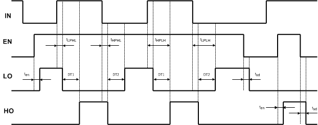 Figure 1. LM5106 Input - Output Waveforms
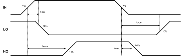 Figure 2. LM5106 Switching Time Definitions: tLPLH, tLPHL, tHPLH, tHPHL
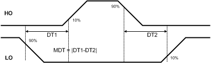 Figure 3. LM5106 Dead-time: DT
6.7 Typical Characteristics
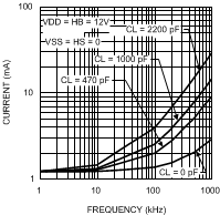 Figure 4. VDD Operating Current vs Frequency
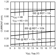 Figure 6. Quiescent Current vs Supply Voltage
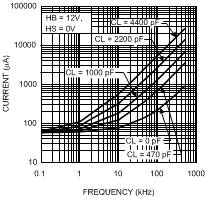 Figure 8. HB Operating Current vs Frequency
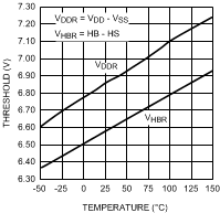 Figure 10. Undervoltage Rising Threshold vs Temperature
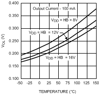 Figure 12. LO and HO - Low-Level Output Voltage vs Temperature
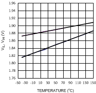 Figure 14. Input Threshold vs Temperature
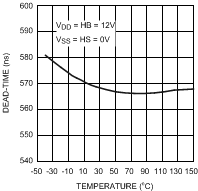 Figure 16. Dead-Time vs Temperature (RT = 100k)
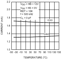 Figure 5. Operating Current vs Temperature
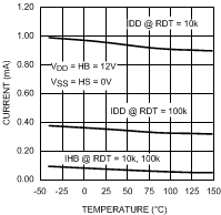 Figure 7. Quiescent Current vs Temperature
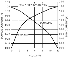 Figure 9. HO and LO Peak Output Current vs Output Voltage
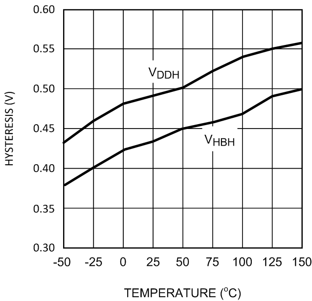 Figure 11. Undervoltage Hysteresis vs Temperature
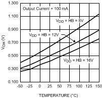 Figure 13. LO and HO - High-Level Output Voltage vs Temperature
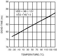 Figure 15. Dead-Time vs Temperature (RT = 10k)
7 Detailed Description
7.1 Overview
The LM5106 is a single PWM input gate driver with Enable that offers a programmable dead-time. The dead-time is set with a resistor at the RDT pin and can be adjusted from 100 ns to 600 ns. The wide dead-time programming range provides the flexibility to optimize drive signal timing for a wide range of MOSFETs and applications.
The RDT pin is biased at 3 V and current limited to 1 mA maximum programming current. The time delay generator will accommodate resistor values from 5k to 100k with a dead-time time that is proportional to the RDT resistance. Grounding the RDT pin programs the LM5106 to drive both outputs with minimum dead-time.
7.2 Functional Block Diagram
7.3 Feature Description
7.3.1 Start-up and UVLO
Both top and bottom drivers include undervoltage lockout (UVLO) protection circuitry which monitors the supply voltage (VDD) and bootstrap capacitor voltage (HB – HS) independently. The UVLO circuit inhibits each driver until sufficient supply voltage is available to turn on the external MOSFETs, and the UVLO hysteresis prevents chattering during supply voltage transitions. When the supply voltage is applied to the VDD pin of the LM5106, the top and bottom gates are held low until VDD exceeds the UVLO threshold, typically about 6.9 V. Any UVLO condition on the bootstrap capacitor will disable only the high-side output (HO).
7.4 Device Functional Modes
| EN | IN Pin | LO Pin | HO Pin |
|---|---|---|---|
| L | Any | L | L |
| H | H | L | H |
| H | L | H | L |
