SLVSBL2D October 2012 – June 2017 TPD5S115
PRODUCTION DATA.
- 1 Features
- 2 Applications
- 3 Description
- 4 Revision History
- 5 Pin Configuration and Functions
-
6 Specifications
- 6.1 Absolute Maximum Ratings
- 6.2 ESD Ratings
- 6.3 Recommended Operating Conditions
- 6.4 Thermal Information
- 6.5 Electrical Characteristics
- 6.6 Electrical Characteristics - I/O Capacitances
- 6.7 Switching Characteristics - VCCA = 1.2 V
- 6.8 Switching Characteristics - VCCA = 1.5 V
- 6.9 Switching Characteristics - VCCA = 1.8 V
- 6.10 Switching Characteristics - VCCA = 2.5 V
- 6.11 Switching Characteristics - VCCA = 3.3 V
- 6.12 Typical Characteristics
- 7 Detailed Description
- 8 Application and Implementation
- 9 Power Supply Recommendations
- 10Layout
- 11Device and Documentation Support
- 12Mechanical, Packaging, and Orderable Information
1 Features
- Conforms to HDMI Compliance Tests Without Any External Components
- Supports HDMI 2.0, HDMI 1.4, and HDMI 1.3 Standards
- Matches HDMI Connector Pin Mapping
- Internal DC-DC Converter to Generate 5 V From a Battery Voltage as Low as 2.3 V
- Auto-Direction Sensing, Level Shifting, and Buffering in the CEC, SDA, and SCL Paths
- IEC 61000-4-2 (Level 4) System Level ESD Compliance
- Reverse Current Blocking and Short-Circuit Protection to Protect Against Fault Conditions
- Industrial Temperature Range: –40°C to 85°C
2 Applications
- Set-Top Boxes
- TVs
- Smart Phones
- Digital Camcorders
- Portable Game Consoles
- Digital Still Cameras
3 Description
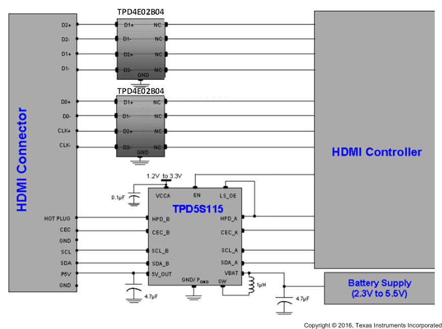
The TPD5S115 device is an integrated HDMI companion chip solution. The device provides a regulated 5-V output (5VOUT) for sourcing the HDMI power line. The regulated 5-V output supplies up to 55 mA to the HDMI receiver with a current limiting function. The TPD5S115 features two control signals: EN and LS_OE. The control of 5VOUT and the hot plug detect (HPD) circuitry is independent of the LS_OE control signal and is controlled by the EN pin. The EN pin allows the detection scheme (5VOUT + HPD) to be active before turning on the whole HDMI link. The LS_OE activates the internal LDO, CEC, SCL, and SDA buffers only when EN is also activated. This dual stage enable scheme ensures optimized power saving for portable applications.
There are three noninverting, bidirectional, voltage level translation circuits for the SDA, SCL, and CEC lines. Each have a common power rail (VCCA) on the A side from 1.1 V to 3.6 V. On the B side, the SCL_B and SDA_B each have an internal 1.75-kΩ pullup connected to the regulated 5-V rail (5VOUT). The DDC (SCL_B and SDA_B) pins meet the I2C specification and drive up to 750-pF loads with the buffers. The CEC_B pin has an internal 27-kΩ pullup to an internal 3.3-V supply. The TPD5S115 exceeds the IEC61000-4-2 (Level 4) ESD protection level. This device features a space saving, 1.72-mm × 1.72-mm, YFF package with 0.4-mm pitch.
Device Information(1)
| PART NUMBER | PACKAGE | BODY SIZE (NOM) |
|---|---|---|
| TPD5S115 | DSBGA (16) | 1.72 mm × 1.72 mm |
- For all available packages, see the orderable addendum at the end of the data sheet.
Typical System Diagram
