-
TS3A5223 0.45 Ω 2-Channel SPDT Bidirectional Analog Switch
- 1 Features
- 2 Applications
- 3 Description
- 4 Revision History
- 5 Pin Configuration and Functions
- 6 Specifications
- 7 Parameter Measurement Information
- 8 Detailed Description
- 9 Application and Implementation
- 10Power Supply Recommendations
- 11Layout
- 12Device and Documentation Support
- 13Mechanical, Packaging, and Orderable Information
- IMPORTANT NOTICE
TS3A5223 0.45 Ω 2-Channel SPDT Bidirectional Analog Switch
1 Features
- Low ON Resistance Switches
- 0.45 Ω (Typical) at 3.6 V
- 0.85 Ω (Typical) at 1.8 V
- Wide Supply Range: 1.65 V to 3.6 V
- 1.0 V Compatible Logic Interface
- High Switch Bandwidth 80 MHz
- 0.01% THD Across Entire Band
- Specified min Break-before-make
- Bi-directional Switching
- –75 dB Channel-to-Channel Crosstalk
- –70 dB Channel-to-Channel OFF Isolation of Very Low Power Dissipation and Leakage Currents
- Very Small QFN-10 Package: 1.8 mm × 1.4 mm
- ESD Protection on all Pins
- 2 kV HBM, 500 V CDM
2 Applications
- Portable Electronics
- Smartphones, Tablets
- Home Electronics
- Wireline Communication
3 Description
The TS3A5223 is a high-speed 2-channel analog switch with break-before-make and bi-directional signal switching capability. The TS3A5223 can be used as a dual 2:1 multiplexer or a 1:2 dual de-multiplexer.
The TS3A5223 offers very low ON resistance, very low THD, channel-to-channel crosstalk and very high OFF isolation. These features make TS3A5223 suitable for application in Audio signal routing and switching applications.
The TS3A5223 control logic supports 1 V – 3.6 V CMOS logic levels. The logic interface allows direct interface with a wide range of CPUs and microcontrollers without increasing the current drawn from supply (ICC) and thus lowering power consumption.
Device Information(1)
| PART NUMBER | PACKAGE | BODY SIZE (NOM) |
|---|---|---|
| TS3A5223 | µQFN (10) | 1.80 mm x 1.40 mm |
- For all available packages, see the orderable addendum at the end of the data sheet.
Functional Diagram

4 Revision History
Changes from A Revision (February 2013) to B Revision
- Added the Device Information table, ESD Ratings table, Thermal Information table, Feature Description section, Device Functional Modes, Application and Implementation section, Power Supply Recommendations section, Layout section, Device and Documentation Support section, and Mechanical, Packaging, and Orderable Information sectionGo
- Changed the VMax MAX value From: 3.6 V To: VCC in the Recommended Operating Conditions tableGo
- Deleted: "dt/dv, SEL pin Input rise and fall time limit" from the Recommended Operating Conditions tableGo
- Deleted the Dissipation Ratings tableGo
Changes from * Revision (January 2013) to A Revision
- Changed the device status From: Preview To: Production Go
5 Pin Configuration and Functions
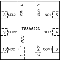
Pin Functions
| NAME | PIN NUMBER | DESCRIPTION | |
|---|---|---|---|
| VCC | 1 | Positive supply Input – Connect 1.65 V to 3.6 V supply voltage | |
| NC1 | 5 | Signal path Input/Output signal pins | |
| NO1 | 2 | ||
| NC2 | 7 | ||
| NO2 | 10 | ||
| COM1, COM2 | 3, 9 | Common signal path Input/Output signal pins | |
| GND | 6 | Ground reference pin | |
| SEL1, SEL2 | 4, 8 | Select digital logic pin. Logic low connects COM to NC, Logic high connects COM to NO | |
6 Specifications
6.1 Absolute Maximum Ratings(1)
Specified at TA= –40°C to 85°C unless otherwise noted.| VALUE | UNIT | ||||
|---|---|---|---|---|---|
| MIN | MAX | ||||
| VCC | Positive DC supply voltage | –0.3 | 4.3(2) | V | |
| VCOM
VNO VNC |
Analog voltage | –0.3 | 4.3(2) | V | |
| ICOM
INO INC |
On-state switch continuous current | ±300 | mA | ||
| ICOM
INO INC |
On-state switch peak current (1ms pulse at 10% duty cycle) | ±500 | mA | ||
| PD | Total device power dissipation at TA = 85°C |
10-µQFN RSW | 430 | mW | |
| TA | Operating free-air ambient temperature range | –40 | 85 | °C | |
| TJ | Junction temperature range | –55 | 150 | °C | |
| Tstg | Storage temperature range | –55 | 150 | °C | |
6.2 ESD Ratings
| VALUE | UNIT | |||
|---|---|---|---|---|
| V(ESD) | Electrostatic discharge | Human-body model (HBM), per ANSI/ESDA/JEDEC JS-001(1) | ±2000 | V |
| Charged-device model (CDM), per JEDEC specification JESD22-C101(2) | ±500 | |||
6.3 Recommended Operating Conditions
over operating free-air temperature range (unless otherwise noted)| MIN | MAX | UNIT | |||
|---|---|---|---|---|---|
| VCC | Positive DC supply voltage | 1.65 | 3.6 | V | |
| VCOM, VNO, VNC | Analog voltage range | 0 | VCC | V | |
| VSEL1
VSEL2 |
Digital logic voltage | 0 | VCC | V | |
| TA | Operating free-air ambient temperature range | –40 | 85 | ºC | |
6.4 Thermal Information
| THERMAL METRIC(1) | TS3A5223 | UNIT | |
|---|---|---|---|
| RSW (UQFN) | |||
| 10 PINS | |||
| RθJA | Junction-to-ambient thermal resistance | 92.5 | °C/W |
| RθJC(top) | Junction-to-case (top) thermal resistance | 46.0 | °C/W |
| RθJB | Junction-to-board thermal resistance | 44.5 | °C/W |
| ψJT | Junction-to-top characterization parameter | 1.5 | °C/W |
| ψJB | Junction-to-board characterization parameter | 44.5 | °C/W |
| RθJC(bot) | Junction-to-case (bottom) thermal resistance | 31.2 | °C/W |
6.5 Electrical Characteristics
Specified over the recommended junction temperature range TA = TJ = –40°C to 85°C Typical values are at TA= TJ = 25°C (unless otherwise noted).| PARAMETER | VCC (V) | TEST CONDITIONS | MIN | TYP | MAX | UNIT | |
|---|---|---|---|---|---|---|---|
| DC CHARACTERISTICS | |||||||
| VIH | High-level Input voltage SEL1, SEL2 inputs | 3.6 | 0.8 | V | |||
| 2.3 | 0.8 | ||||||
| 1.8 | 0.8 | ||||||
| VIL | Low-level Input voltage SEL1, SEL2 inputs | 3.6 | 0.3 | V | |||
| 2.3 | 0.3 | ||||||
| 1.8 | 0.3 | ||||||
| RON | Switch ON Resistance | 3.6 | VS = 0 to VCC, IS = 100 mA, VSEL = 1 V, 0 V |
0.45 | 0.6 | Ω | |
| 2.3 | 0.6 | 0.8 | |||||
| 1.8 | 0.85 | 1.2 | |||||
| ΔRON | Difference of on-state resistance between switches | 3.6 | VS = 2 V, 0.8 V, IS = 100 mA, VSEL = 1 V, 0 V |
0.05 | Ω | ||
| RON-FLAT | ON resistance flatness | 3.6 | VS = 0 to VCC, IS = 100mA, VSEL = 1 V, 0 V |
0.1 | 0.2 | Ω | |
| 2.3 | 0.15 | 0.35 | |||||
| 1.8 | 0.4 | 0.65 | |||||
| IOFF | NC, NO pin leakage current when switch is off | 3.6 | VS = 0.3 or 3.0V, VCOM = 3 or 0.3 V | 5 | 90 | nA | |
| IS(ON) | NC, NO pin leakage current when switch is on | 3.6 | VS = 0.3 or 3.0V, VCOM = No Load | 4 | 60 | nA | |
| ISEL | Select pin input leakage current | VS | VS = 0 or 3.6 V | 100 | nA | ||
| ICC | Quiescent supply current | 3.6 | VSEL = 0 or VCC | 700 | 2000 | nA | |
| ICCLV | Supply current change | 3.6 | VSEL = 1 V to VSEL = VCC | 200 | nA | ||
| SWITCHING PARAMETERS(1)(2) | |||||||
| tPHL | Logic high to low propagation delay | 3.6 | RL = 50 Ω, CL = 35 pF | 0.1 | ns | ||
| 2.5 | 0.2 | ||||||
| 1.8 | 0.2 | ||||||
| tPLH | Logic low to high propagation delay | 3.6 | RL = 50 Ω, CL = 35 pF | 0.1 | ns | ||
| 2.5 | 0.2 | ||||||
| 1.8 | 0.2 | ||||||
| tON | Turn-ON time | 2.3 - 3.6 | RL = 50 Ω, CL = 35 pF, VS = 1.5 V | 70 | ns | ||
| tOFF | Turn-OFF time | 2.3 - 3.6 | RL = 50 Ω, CL = 35 pF, VS = 1.5 V | 75 | ns | ||
| tBBM | Break-before-make time delay | 3.6 | RL = 50 Ω, CL = 35 pF, VS = 1.5 V | 2 | 8 | ns | |
| QINJ | Charge Injection | 3.6 | CL = 1 nF, VS = 0 V | 40 | pC | ||
| AC CHARACTERISTICS | |||||||
| BW | -3 dB Bandwidth | 1.65 - 3.6 | RL = 50 Ω, CL = 35 pF | 80 | MHz | ||
| VISO | Channel OFF isolation | 1.65 - 3.6 | VS = 1 Vrms, f = 100 kHz | –70 | dB | ||
| VXtalk | Channel-to-Channel Crosstalk | 1.65 - 3.6 | VS = 1 Vrms, f = 100kHz | –75 | dB | ||
| THD | Total harmonic distortion | 1.65 - 3.6 | RL = 600 Ω, VSEL = 2 Vpk-pk, f = 20 Hz to 20 kHz |
0.01% | |||
| CSEL | Select pin input capacitance | 3.3 | f = 1 MHz | 3 | pF | ||
| CON | NC, NO, and COM input capacitance when switch is on | 3.3 | f = 1 MHz | 115 | pF | ||
| COFF | NC, NO, and COM input capacitance when switch is off | 3.3 | f = 1 MHz | 50 | pF | ||
6.6 Typical Characteristics

| VCC = 1.8 V |

| VCC = 3 V |

| TA = 25°C |

| VCC = 2.3 V |

| VCC = 3.6 V |

7 Parameter Measurement Information
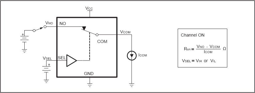 Figure 7. ON-State Resistance (RON)
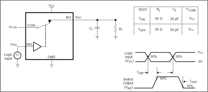 Figure 8. Turn-On (tON) and Turn-Off Time (tOFF)
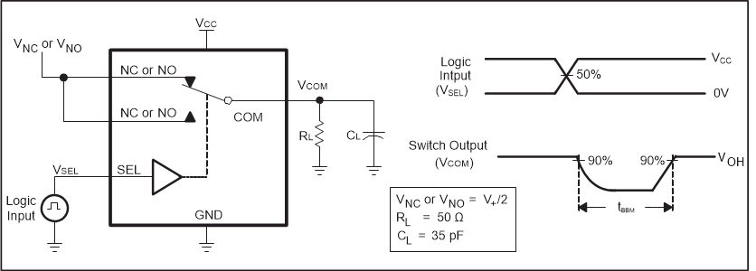 Figure 9. Break-Before-Make Time (tBBM)
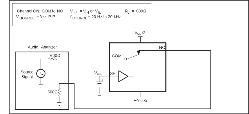 Figure 10. TOTAL HARMONIC DISTORTION (THD)
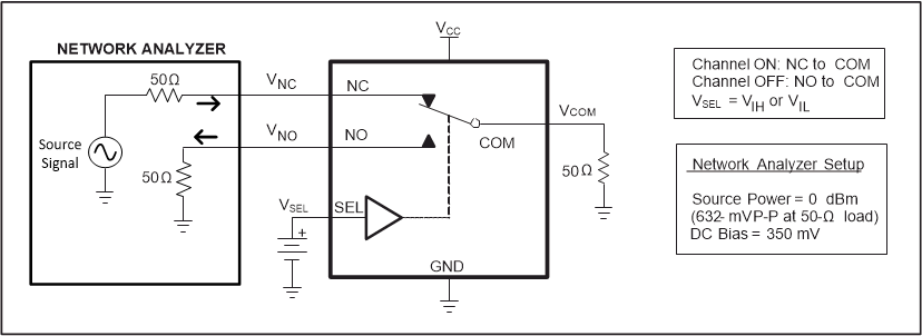 Figure 11. Crosstalk (XTALK)
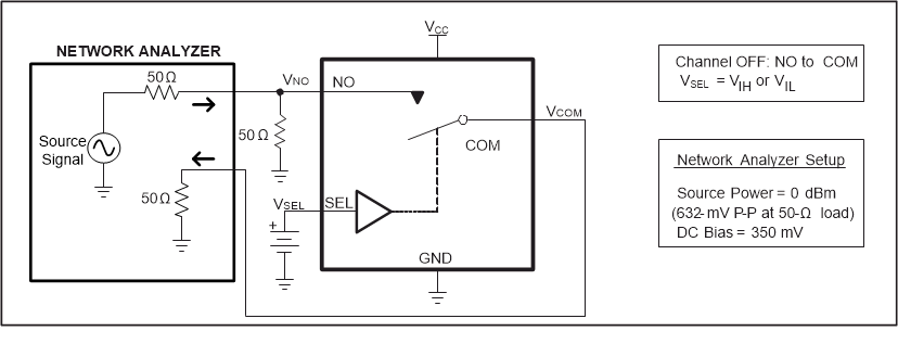 Figure 12. OFF Isolation (OISO)