SLUSBD8E February 2013 – December 2014 UCC28251
PRODUCTION DATA.
- 1 Features
- 2 Applications
- 3 Description
- 4 Revision History
- 5 Description (continued)
- 6 Pin Configuration and Functions
- 7 Specifications
-
8 Detailed Description
- 8.1 Overview
- 8.2 Functional Block Diagram
- 8.3
Feature Description
- 8.3.1 VDD (5/12)
- 8.3.2 VREF (Reference Generator) (20/7)
- 8.3.3 EN (Enable Pin) (18/5)
- 8.3.4 RT (Oscillator Frequency Set and Synchronization) (15/2)
- 8.3.5 SP (Synchronous Rectifier Turn-Off to Primary Output Turn-On Dead Time Programming) (13/19)
- 8.3.6 PS (Primary Output Turn-Off to Synchronous Rectifier Turn-On Dead Time Programming) (11/18)
- 8.3.7 RAMP/CS (PWM Ramp Input or Current Sense Input) (16/3)
- 8.3.8 REF/EA+ (1/8)
- 8.3.9 FB/EA- (2/9)
- 8.3.10 COMP (3/10)
- 8.3.11 VSENSE (14/1)
- 8.3.12 SS (Soft Start Programming Pin) (13/20)
- 8.3.13 ILIM (Current Limit for Cycle-by-Cycle Over-Current Protection) (17/4)
- 8.3.14 HICC (10/17)
- 8.3.15 OVP/OTP (19/6)
- 8.3.16 OUTA (9/16) and OUTB (8/15)
- 8.3.17 SRA (7/14) and SRB (6/13)
- 8.3.18 GND (4/11)
- 8.4 Device Functional Modes
-
9 Application and Implementation
- 9.1 Application Information
- 9.2
Typical Applications
- 9.2.1
Circuit Diagram in Design Example
- 9.2.1.1 Design Requirements
- 9.2.1.2
Detailed Design Procedure
- 9.2.1.2.1 Step 1: Power Stage Design
- 9.2.1.2.2 Step 2: Feedback Loop Design
- 9.2.1.2.3 Step 3: Programming The Device
- 9.2.1.2.4 Step 3-3: Determine Soft-Start Capacitance
- 9.2.1.2.5 Step 3-4: Determine Dead-Time Resistance
- 9.2.1.2.6 Step 3-5: Determine OCP Hiccup Off-Time Capacitance
- 9.2.1.2.7 Step 3-6: Determine Primary-Side OVP Resistance
- 9.2.1.2.8 Step 3-7: Select Capacitance for VDD and VREF
- 9.2.1.3 Application Curves
- 9.2.2 Secondary-Side Half-Bridge Controller With Synchronous Rectification
- 9.2.1
Circuit Diagram in Design Example
- 10Power Supply Recommendations
- 11Layout
- 12Device and Documentation Support
- 13Mechanical, Packaging, and Orderable Information
パッケージ・オプション
メカニカル・データ(パッケージ|ピン)
サーマルパッド・メカニカル・データ
- RGP|20
発注情報
1 Features
- Prebiased Startup
- Synchronous Rectifier Control Outputs with Programmable Delays (Including Zero Delay Support)
- Voltage Mode Control with Input Voltage Feed-Forward or Current Mode Control
- Primary or Secondary-Side Control
- 3.3-V, 1.5% Accurate Reference Output
- Lower Minimum Operating Frequency
- 1% Accurate Cycle-by-Cycle Over Current Protection with Matched Duty Cycle Outputs
- Programmable Soft-Start and Hiccup Restart Timer
- Thermally Enhanced 4-mm x 4-mm VQFN-20 Package and 20-pin TSSOP Package
2 Applications
- Half-Bridge, Full-Bridge, Interleaved Forward, and Push-Pull Isolated Converters
- Telecom and Data-com Power
- Wireless Base Station Power
- Server Power
- Industrial Power Systems
3 Description
The UCC28251 PWM controller is designed for high power density applications that may have stringent prebiased startup requirements. The UCC28251’s integrated synchronous rectifier control outputs target high efficiency and high performance topologies such as half-bridge, full-bridge, interleaved forward, and push-pull. The UCC27210 half bridge drivers and UCC2752x MOSFET drivers used in conjunction with the UCC28251 provide a complete power converter solution.
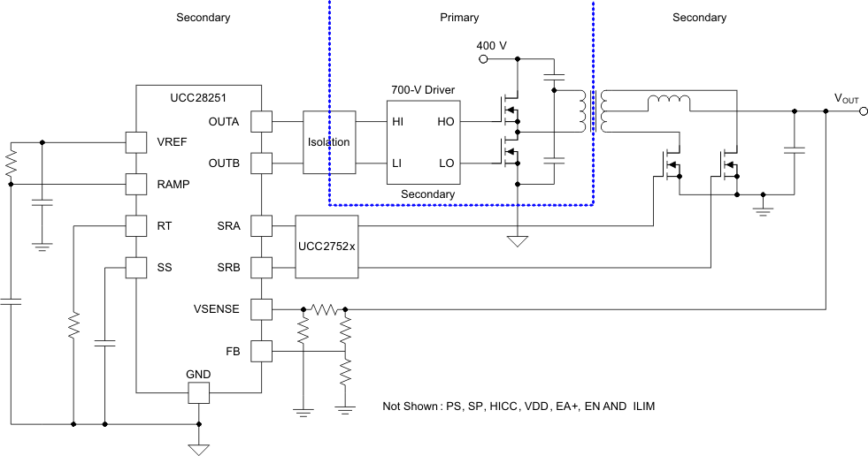
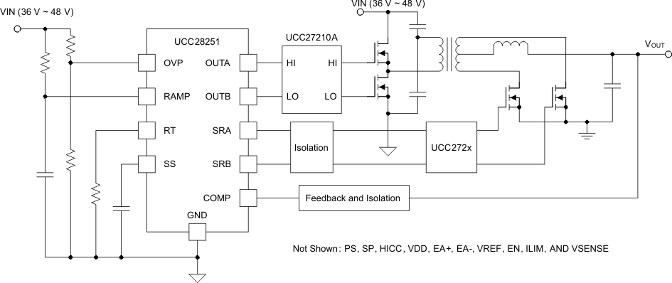
The UCC28251 is a functional variant of the UCC28250 PWM Controller. While the same basic functionality of the UCC28250 is largely maintained, the UCC28251 is designed to enhance performance in both offline, 400-V input DC-to-DC applications and 48-V input full-bridge or half-bridge applications.
Device Information(1)
| PART NUMBER | PACKAGE | BODY SIZE (NOM) |
|---|---|---|
| UCC28251 | TSSOP (20) | 6.50 mm × 4.40 mm |
| VQFN (20) | 4.00 mm × 4.00 mm |
- For all available packages, see the orderable addendum at the end of the datasheet.
Simple Application Diagram (400-VIN DC-to-DC Converter)

Simple Application Diagram (48-VIN DC-to-DC Converter)
