DS90LV047A 3V LVDSクワッドCMOS差動ライン・ドライバ
1 特長
2 アプリケーション
- マルチファンクションのプリンタ
- LVDS - LVCMOS変換
3 概要
DS90LV047Aデバイスは、クワッドCMOSフロースルー差動ライン・ドライバで、非常に低い消費電力と高いデータ速度を必要とするアプリケーション用に設計されています。このデバイスは、低電圧差動信号(LVDS)テクノロジを活用し、400Mbps (200MHz)を超えるデータ転送速度をサポートするよう設計されています。
DS90LV047Aは低電圧のTTL/CMOS入力レベルを受け付け、低電圧(350mV)の差動出力信号へ変換します。
さらに、ドライバはTRI-STATE機能をサポートし、出力ステージのディセーブルと負荷電流のディセーブルを行うため、デバイスはアイドル状態で13mW (標準値)と極めて低い消費電力を実現します。DS90LV047Aはフロースルーのピン配置を採用しているため、PCBレイアウトが簡単になります。
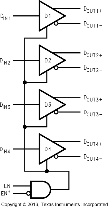
ENおよびEN*入力は互いにAND接続され、TRI-STATE出力を制御します。イネーブルは4つのドライバすべてに共通です。DS90LV047Aおよびコンパニオン・ライン・レシーバ(DS90LV048A)は、消費電力の大きい疑似ECLデバイスの新しい代替品として、高速のポイント・ツー・ポイント・インターフェイス・アプリケーション用に使用できます。
製品情報(1)
| 型番 | パッケージ | 本体サイズ(公称) |
|---|---|---|
| DS90LV048A | SOIC (16) | 9.90mm×3.91mm |
| TSSOP (16) | 5.00mm×4.40mm |
- 提供されているすべてのパッケージについては、データシートの末尾にある注文情報を参照してください。
機能図
4 改訂履歴
Changes from C Revision (April 2013) to D Revision
- 「ESD定格」の表、「熱に関する情報」セクション、「機能説明」セクション、「デバイスの機能モード」セクション、「アプリケーションと実装」セクション、「電源に関する推奨事項」セクション、「レイアウト」セクション、「デバイスおよびドキュメントのサポート」セクション、「メカニカル、パッケージ、および注文情報」セクションを追加Go
Changes from B Revision (April 2013) to C Revision
- Changed layout of National Semiconductor Data Sheet to TI formatGo
5 Pin Configuration and Functions

Pin Functions
| PIN | I/O | DESCRIPTION | |
|---|---|---|---|
| NAME | NO. | ||
| DIN | 2, 3, 6, 7 | I | Driver input pin, TTL/CMOS compatible |
| DOUT+ | 10, 11, 14, 15 | O | Non-inverting driver output pin, LVDS levels |
| DOUT− | 9, 12, 13, 16 | O | Inverting driver output pin, LVDS levels |
| EN | 1 | I | Driver enable pin: When EN is low, the driver is disabled. When EN is high and EN* is low or open, the driver is enabled. If both EN and EN* are open circuit, then the driver is disabled. |
| EN* | 8 | I | Driver enable pin: When EN* is high, the driver is disabled. When EN* is low or open and EN is high, the driver is enabled. If both EN and EN* are open circuit, then the driver is disabled. |
| GND | 5 | — | Ground pin |
| VCC | 4 | — | Power supply pin, +3.3 V ± 0.3 V |
6 Specifications
6.1 Absolute Maximum Ratings
See (1)| MIN | MAX | UNIT | |||
|---|---|---|---|---|---|
| Supply voltage (VCC) | −0.3 | 4 | V | ||
| Input voltage (DIN) | −0.3 | VCC + 0.3 | V | ||
| Enable input voltage (EN, EN*) | −0.3 | VCC + 0.3 | V | ||
| Output voltage (DOUT+, DOUT–) | −0.3 | 3.9 | V | ||
| Short-circuit duration | (DOUT+, DOUT–) | Continuous | |||
| Maximum package power dissipation at +25°C | D0016A package | 1088 | mW | ||
| PW0016A package | 866 | ||||
| Derate D0016A package | above +25°C | 8.5 | mW/°C | ||
| Derate PW0016A package | above +25°C | 6.9 | |||
| Lead temperature | Soldering (4 s) | 260 | °C | ||
| Maximum junction temperature | 150 | °C | |||
| Storage temperature, Tstg | −65 | 150 | °C | ||
6.2 ESD Ratings
| VALUE | UNIT | |||
|---|---|---|---|---|
| V(ESD) | Electrostatic discharge(1) | Human-body model (HBM) | ±10000 | V |
| Machine Model | ±1200 | |||
HBM (1.5 kΩ, 100 pF)
EIAJ (0 Ω, 200 pF)
6.3 Recommended Operating Conditions
| MIN | NOM | MAX | UNIT | ||
|---|---|---|---|---|---|
| Supply voltage, VCC | 3 | 3.3 | 3.6 | V | |
| Operating free air temperature, TA | −40 | 25 | 85 | °C | |
6.4 Thermal Information
| THERMAL METRIC(1) | DS90LV047A | UNIT | |
|---|---|---|---|
| PW (TSSOP) | |||
| 16 PINS | |||
| RθJA | Junction-to-ambient thermal resistance | 114 | °C/W |
| RθJC(top) | Junction-to-case (top) thermal resistance | 51 | °C/W |
| RθJB | Junction-to-board thermal resistance | 59 | °C/W |
| ψJT | Junction-to-top characterization parameter | 8 | °C/W |
| ψJB | Junction-to-board characterization parameter | 58 | °C/W |
6.5 Electrical Characteristics
Over supply voltage and operating temperature ranges, unless otherwise specified(1)(2)(3)| PARAMETER | TEST CONDITIONS | PIN | MIN | TYP | MAX | UNIT | |
|---|---|---|---|---|---|---|---|
| VOD1 | Differential output voltage | RL = 100 Ω (Figure 17) | DOUT−
DOUT+ |
250 | 310 | 450 | mV |
| ΔVOD1 | Change in magnitude of VOD1 for complementary output states | 1 | 35 | |mV| | |||
| VOS | Offset voltage | 1.125 | 1.17 | 1.375 | V | ||
| ΔVOS | Change in magnitude of VOS for complementary output states | 1 | 25 | |mV| | |||
| VOH | Output high voltage | 1.33 | 1.6 | V | |||
| VOL | Output low voltage | 0.9 | 1.02 | V | |||
| VIH | Input high voltage | DIN, EN, EN* | 2 | VCC | V | ||
| VIL | Input low voltage | GND | 0.8 | V | |||
| IIH | Input high current | VIN = VCC or 2.5 V | −10 | 2 | +10 | µA | |
| IIL | Input low current | VIN = GND or 0.4 V | −10 | −2 | +10 | µA | |
| VCL | Input clamp voltage | ICL = −18 mA | −1.5 | −0.8 | V | ||
| IOS | Output short-circuit current(4) | ENABLED, DIN = VCC, DOUT+ = 0 V or DIN = GND, DOUT− = 0 V |
DOUT−
DOUT+ |
−4.2 | −9 | mA | |
| IOSD | Differential output short-circuit current(4) | ENABLED, VOD = 0 V | −4.2 | −9 | mA | ||
| IOFF | Power-off leakage | VOUT = 0 V or 3.6 V, VCC = 0 V or Open | −20 | ±1 | 20 | µA | |
| IOZ | Output TRI-STATE current | EN = 0.8 V and EN* = 2.0 V VOUT = 0 V or VCC |
−10 | ±1 | 10 | µA | |
| ICC | No load supply current drivers enabled | DIN = VCC or GND | VCC | 4 | 8 | mA | |
| ICCL | Loaded supply current drivers enabled | RL = 100 Ω all channels, DIN = VCC or GND (all inputs) | 20 | 30 | mA | ||
| ICCZ | No load supply current drivers disabled | DIN = VCC or GND, EN = GND, EN* = VCC |
2.2 | 6 | mA | ||
6.6 Switching Characteristics
VCC = +3.3V ± 10%, TA = −40°C to +85°C(1)(2)(3)| PARAMETER | TEST CONDITIONS | MIN | TYP | MAX | UNIT | |
|---|---|---|---|---|---|---|
| tPHLD | Differential propagation delay high to low | RL = 100 Ω, CL = 15 pF (Figure 18 and Figure 19) |
0.5 | 0.9 | 1.7 | ns |
| tPLHD | Differential propagation delay low to high | 0.5 | 1.2 | 1.7 | ns | |
| tSKD1 | Differential pulse skew |tPHLD − tPLHD|(4) | 0 | 0.3 | 0.4 | ns | |
| tSKD2 | Channel-to-channel skew(5) | 0 | 0.4 | 0.5 | ns | |
| tSKD3 | Differential part-to-part skew(6) | 0 | 1 | ns | ||
| tSKD4 | Differential part-to-part skew(7) | 0 | 1.2 | ns | ||
| tTLH | Rise time | 0.5 | 1.5 | ns | ||
| tTHL | Fall time | 0.5 | 1.5 | ns | ||
| tPHZ | Disable time high to Z | RL = 100 Ω, CL = 15 pF (Figure 20 and Figure 21) |
2 | 5 | ns | |
| tPLZ | Disable time low to Z | 2 | 5 | ns | ||
| tPZH | Enable time Z to high | 3 | 7 | ns | ||
| tPZL | Enable time Z to low | 3 | 7 | ns | ||
| fMAX | Maximum operating frequency(8) | 200 | 250 | MHz | ||
VOD > 250 mV, all channels switching.
6.7 Typical Characteristics
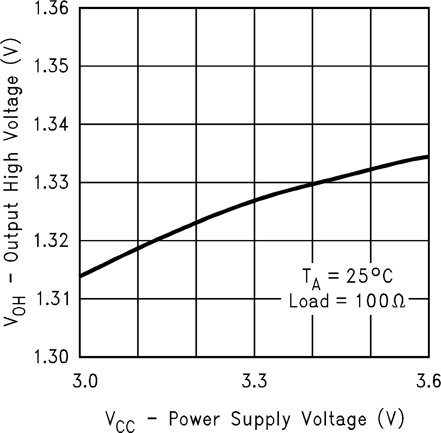 Figure 1. Output High Voltage vs Power Supply Voltage
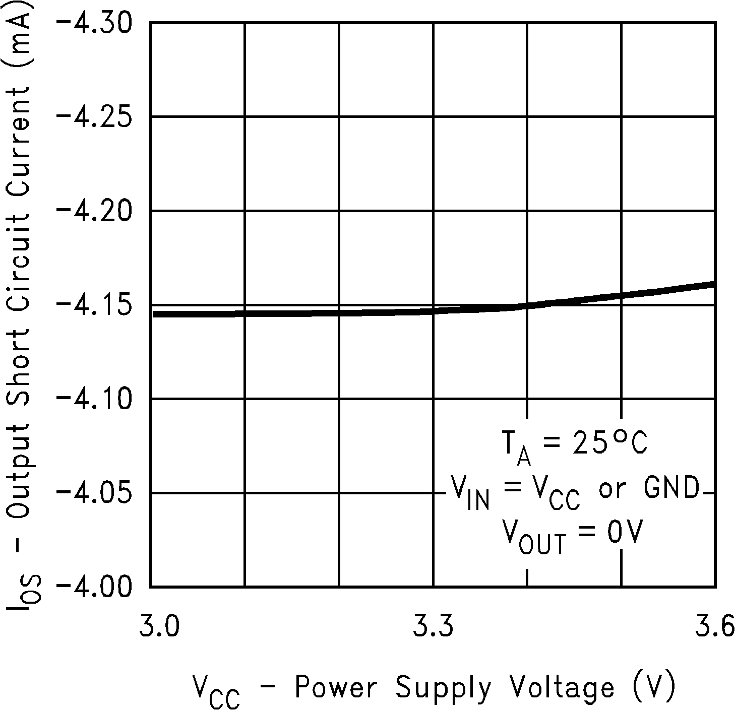 Figure 3. Output Short Circuit Current vs
Power Supply Voltage
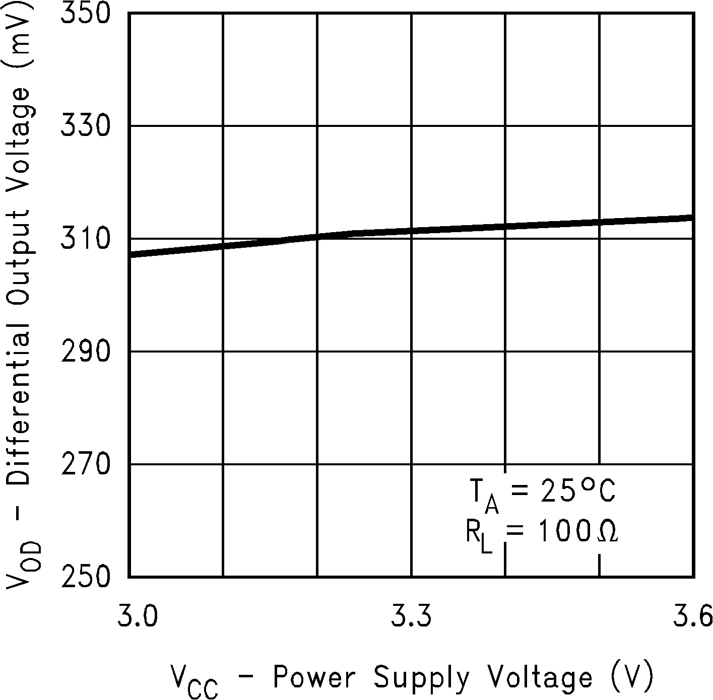 Figure 5. Differential Output Voltage vs
Power Supply Voltage
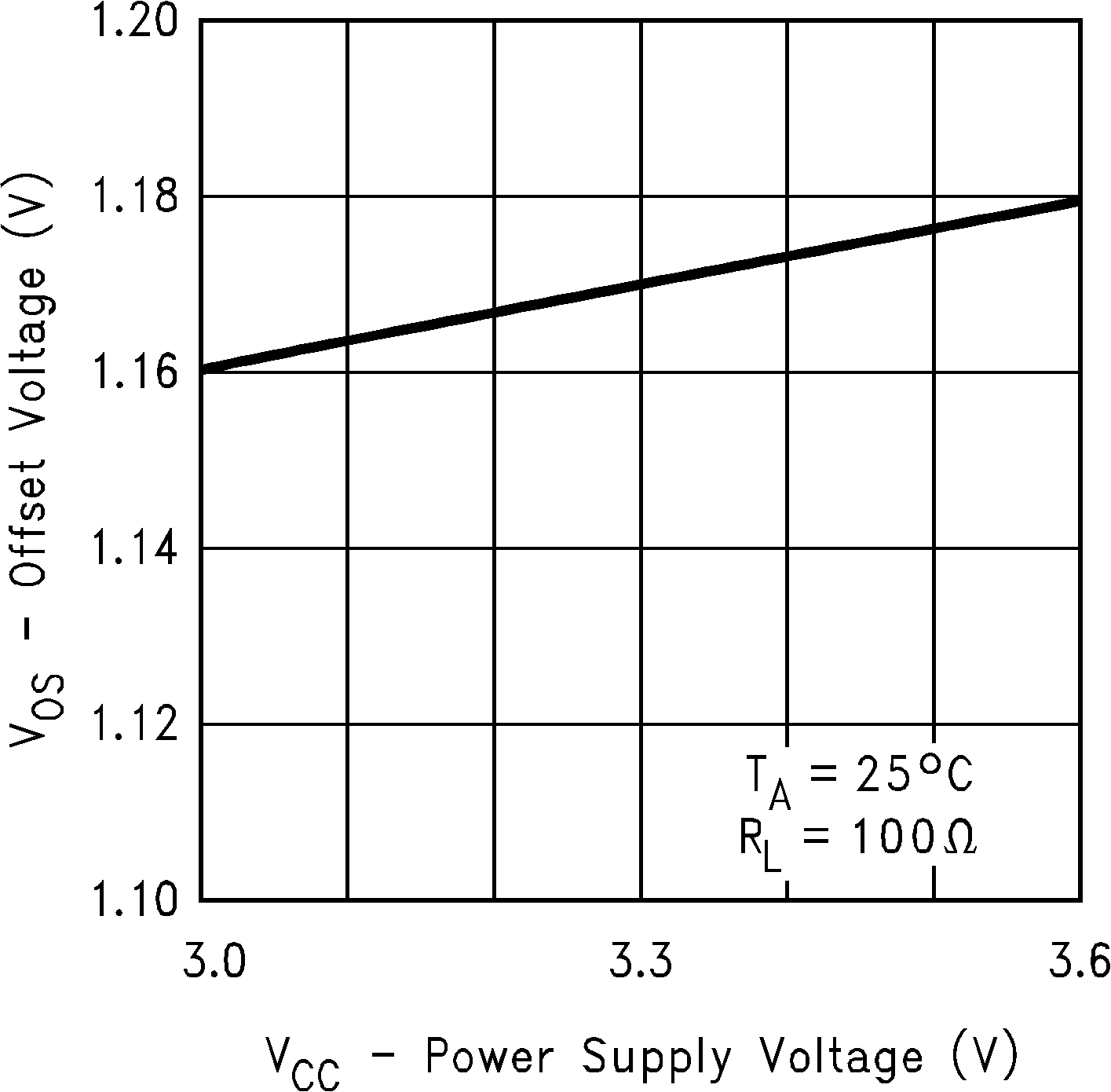 Figure 7. Offset Voltage vs Power Supply Voltage
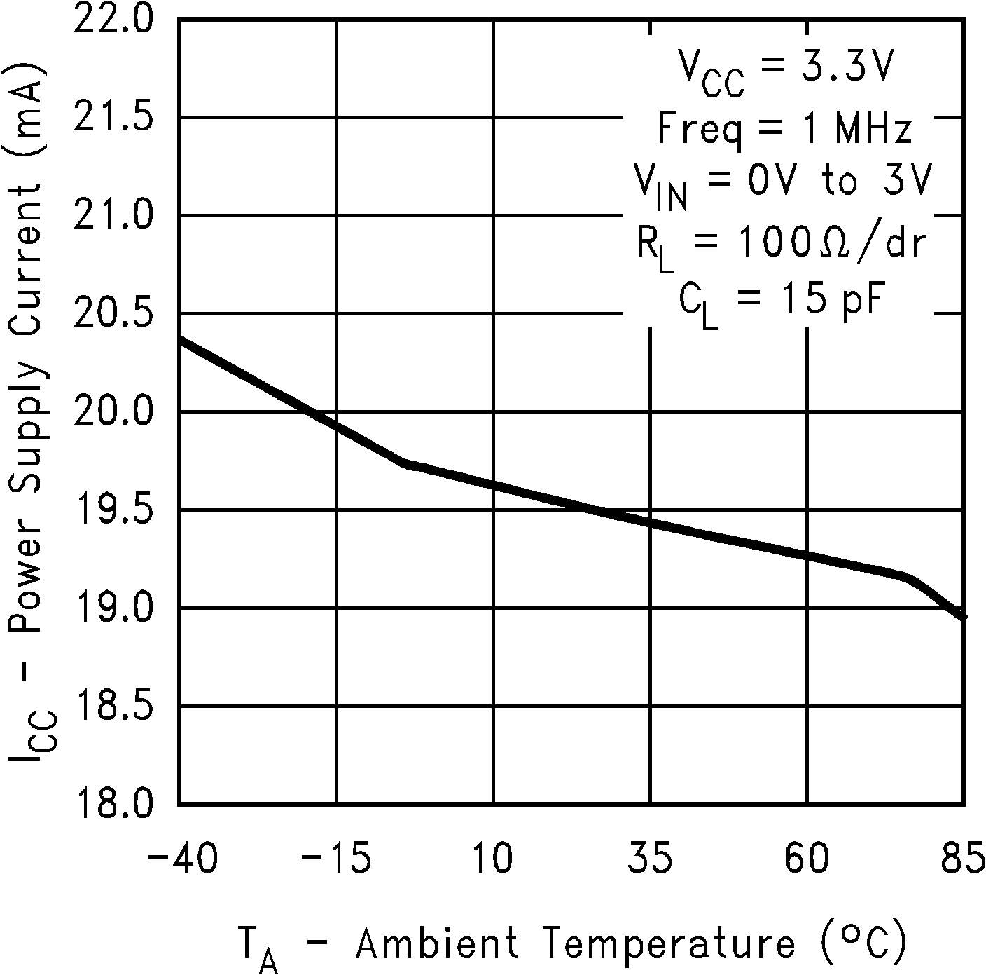 Figure 9. Power Supply Current vs Ambient Temperature
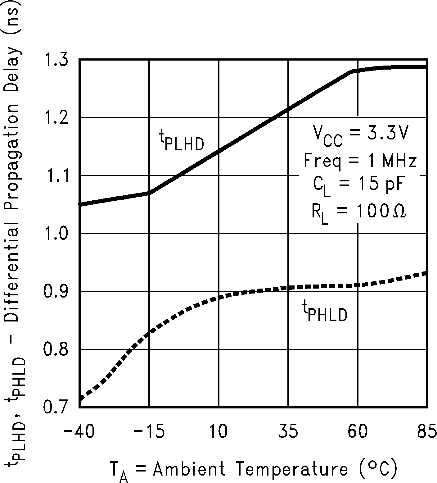 Figure 11. Differential Propagation Delay vs
Ambient Temperature
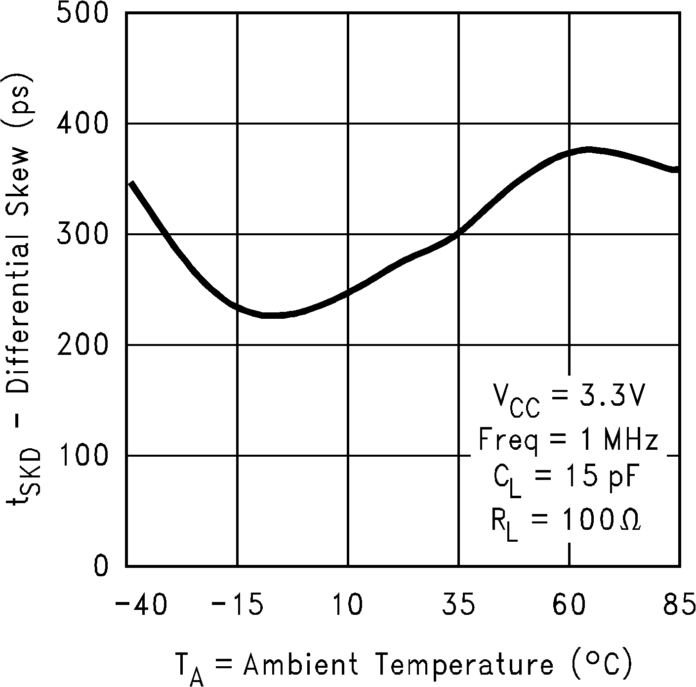 Figure 13. Differential Skew vs Ambient Temperature
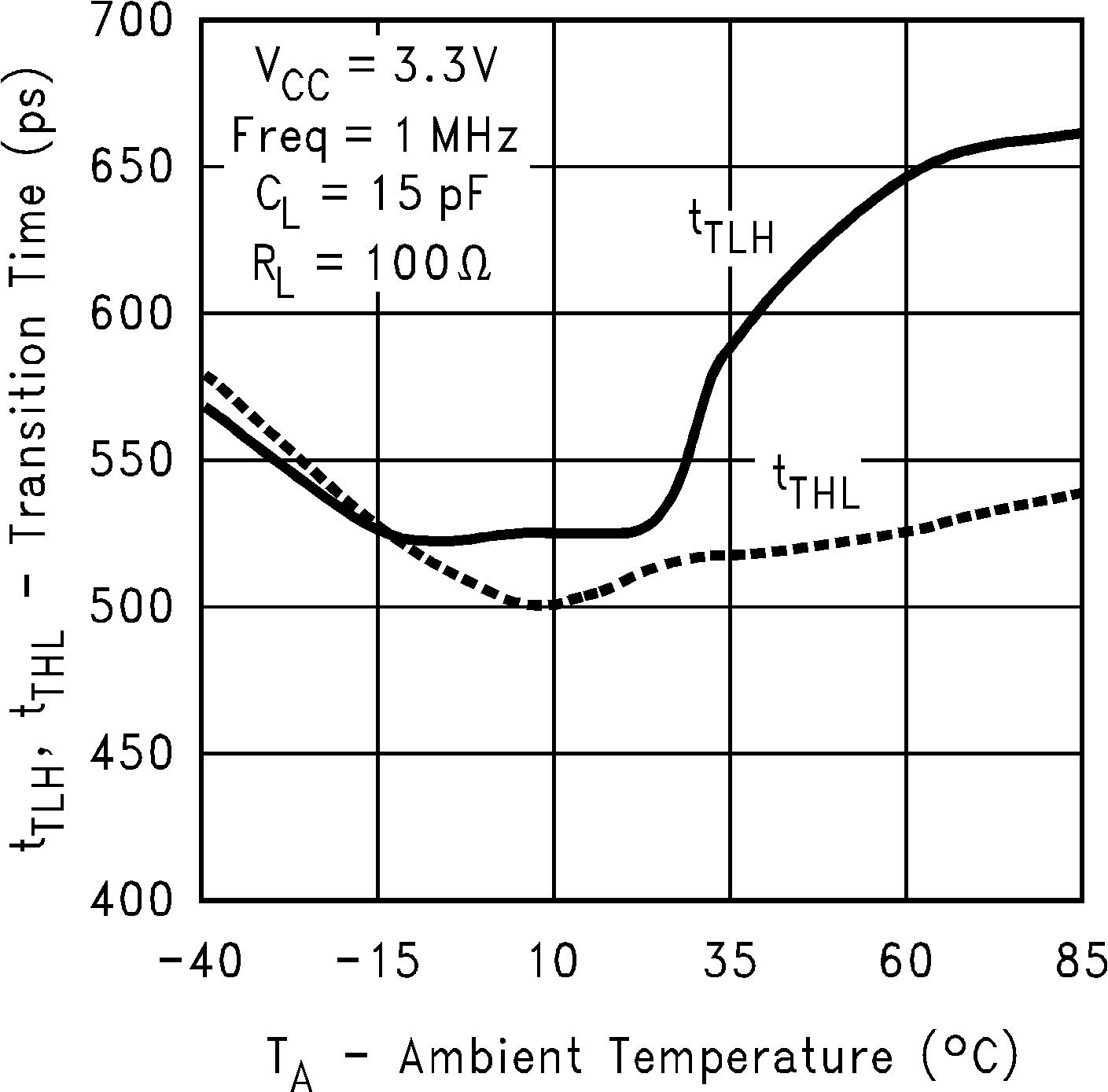 Figure 15. Transition Time vs Ambient Temperature
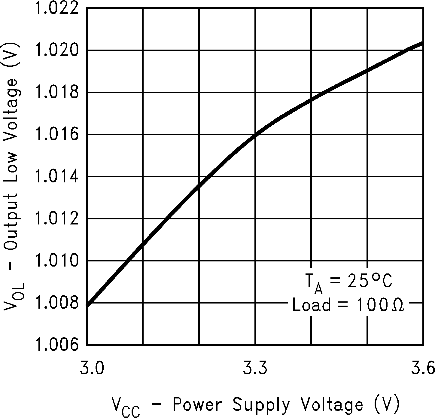 Figure 2. Output Low Voltage vs Power Supply Voltage
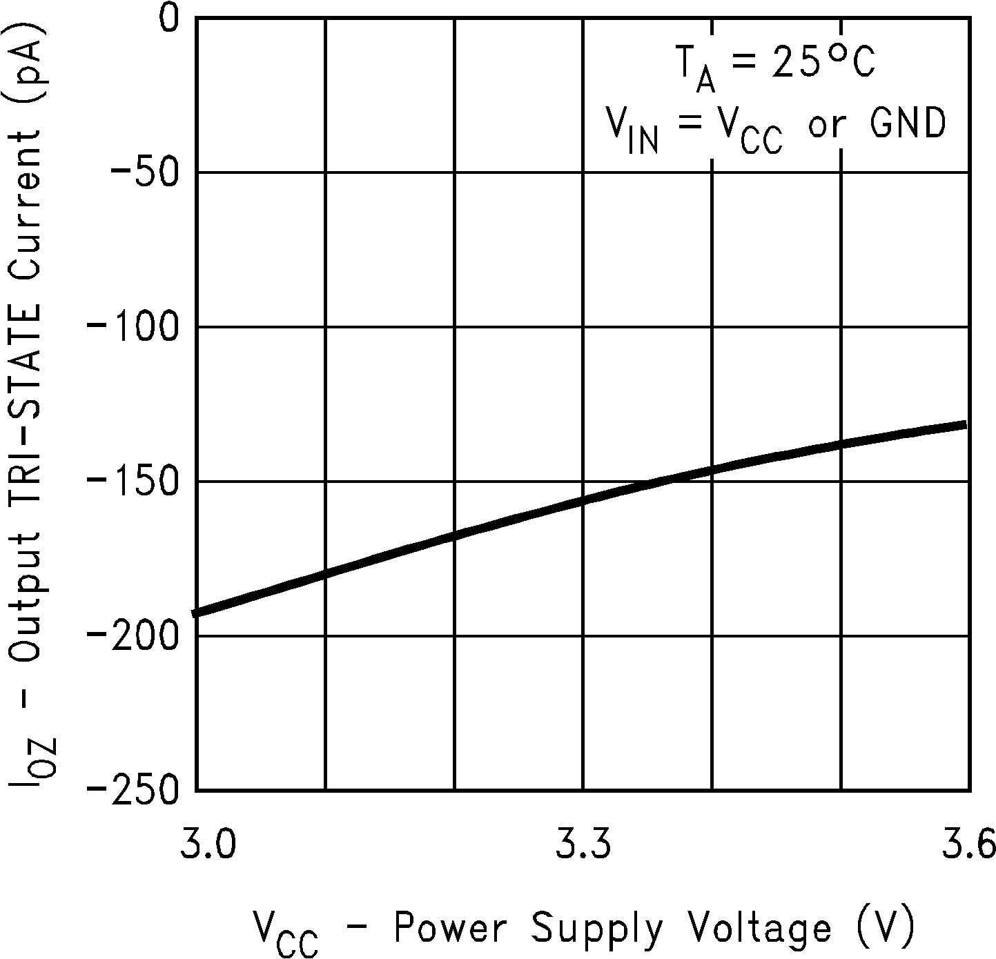 Figure 4. Output TRI-STATE Current vs
Power Supply Voltage
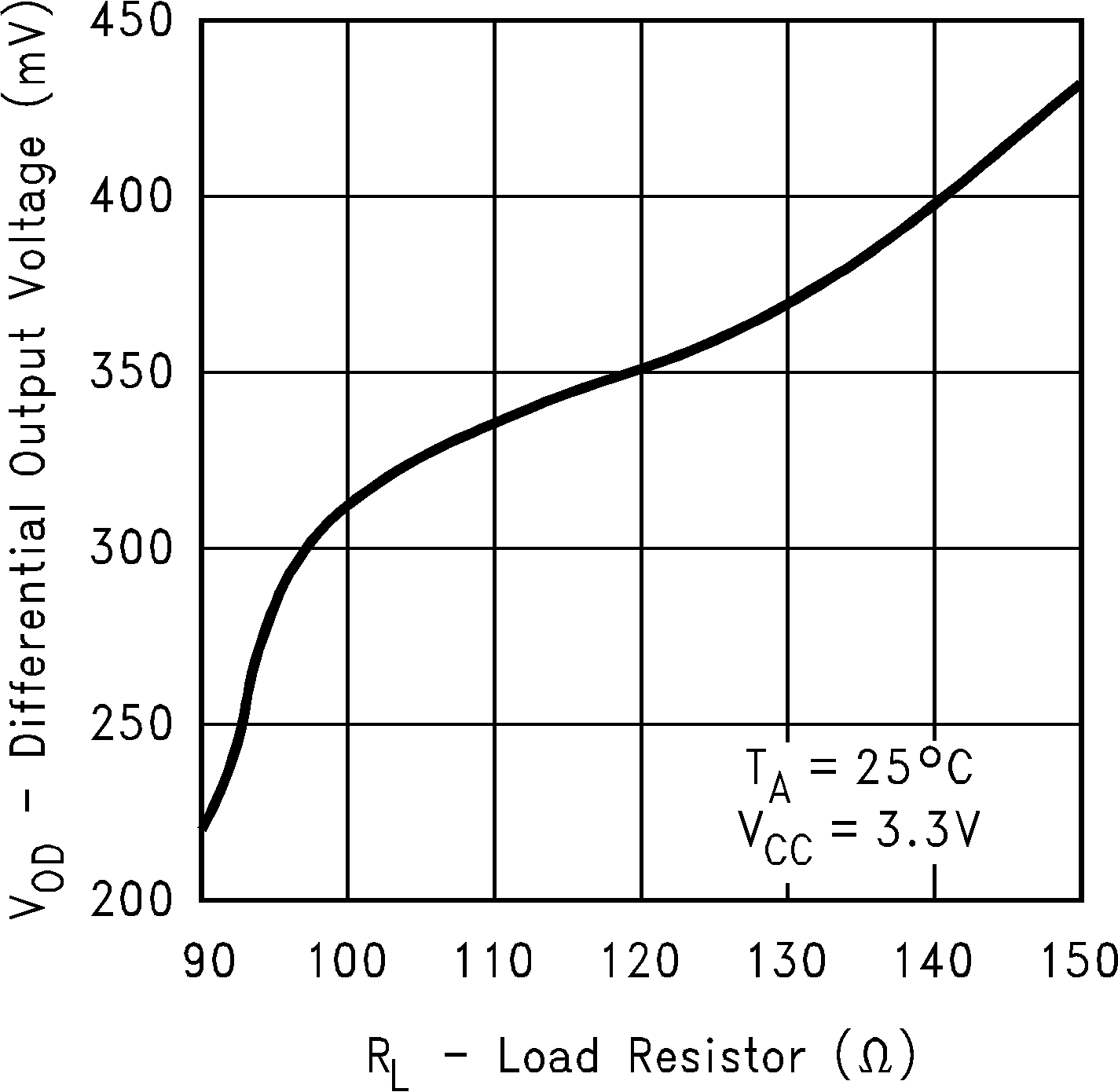 Figure 6. Differential Output Voltage vs Load Resistor
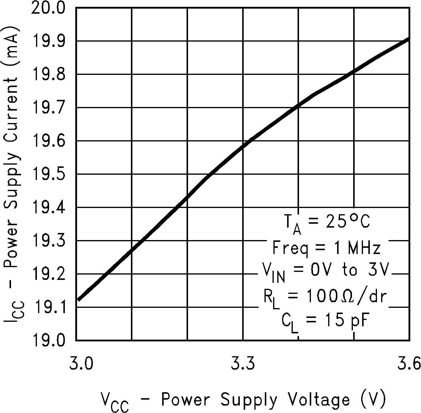 Figure 8. Power Supply Current vs Power Supply Voltage
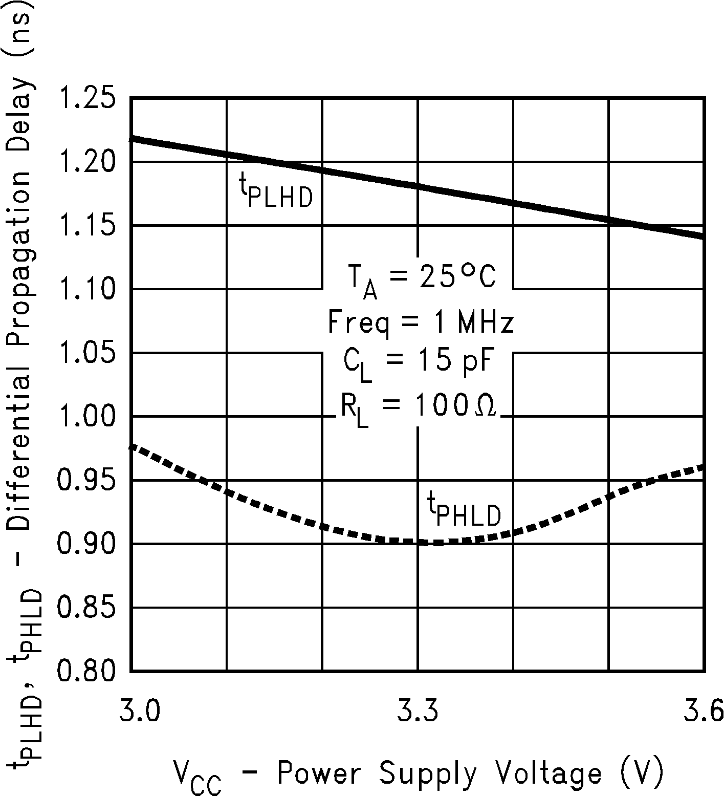 Figure 10. Differential Propagation Delay vs
Power Supply Voltage
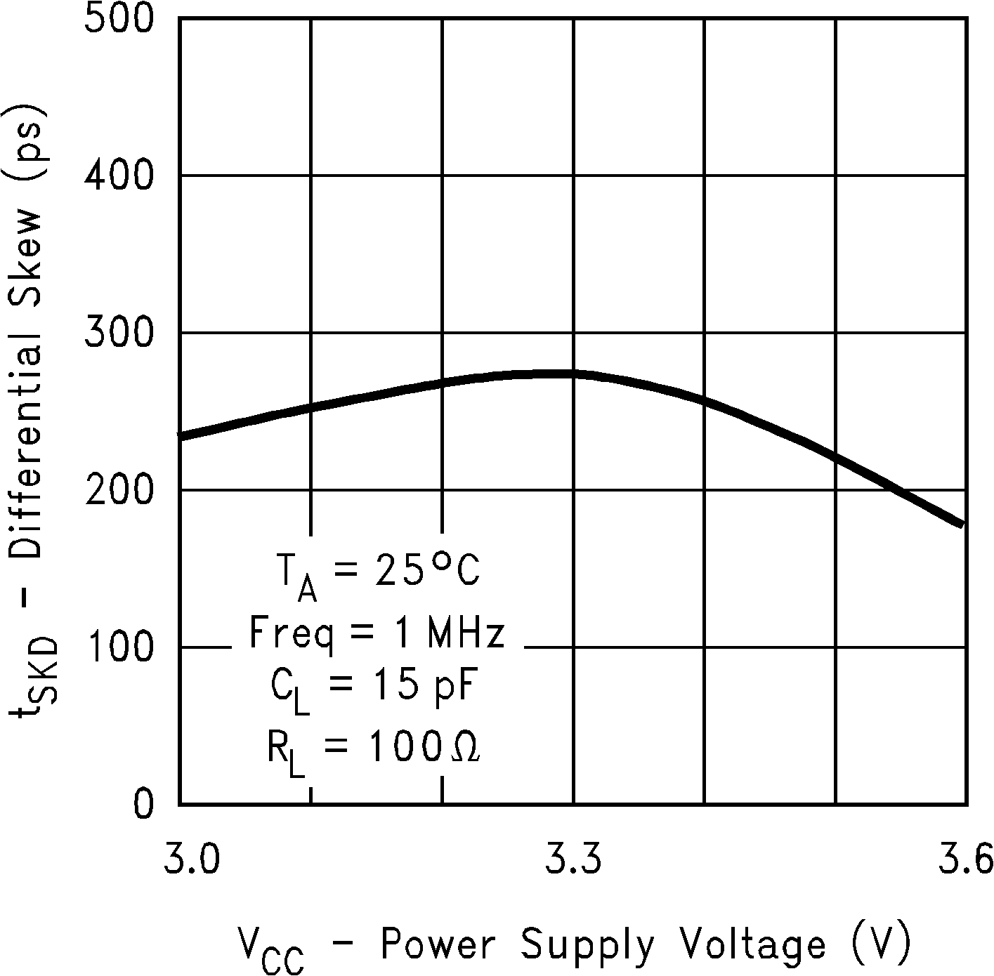 Figure 12. Differential Skew vs Power Supply Voltage
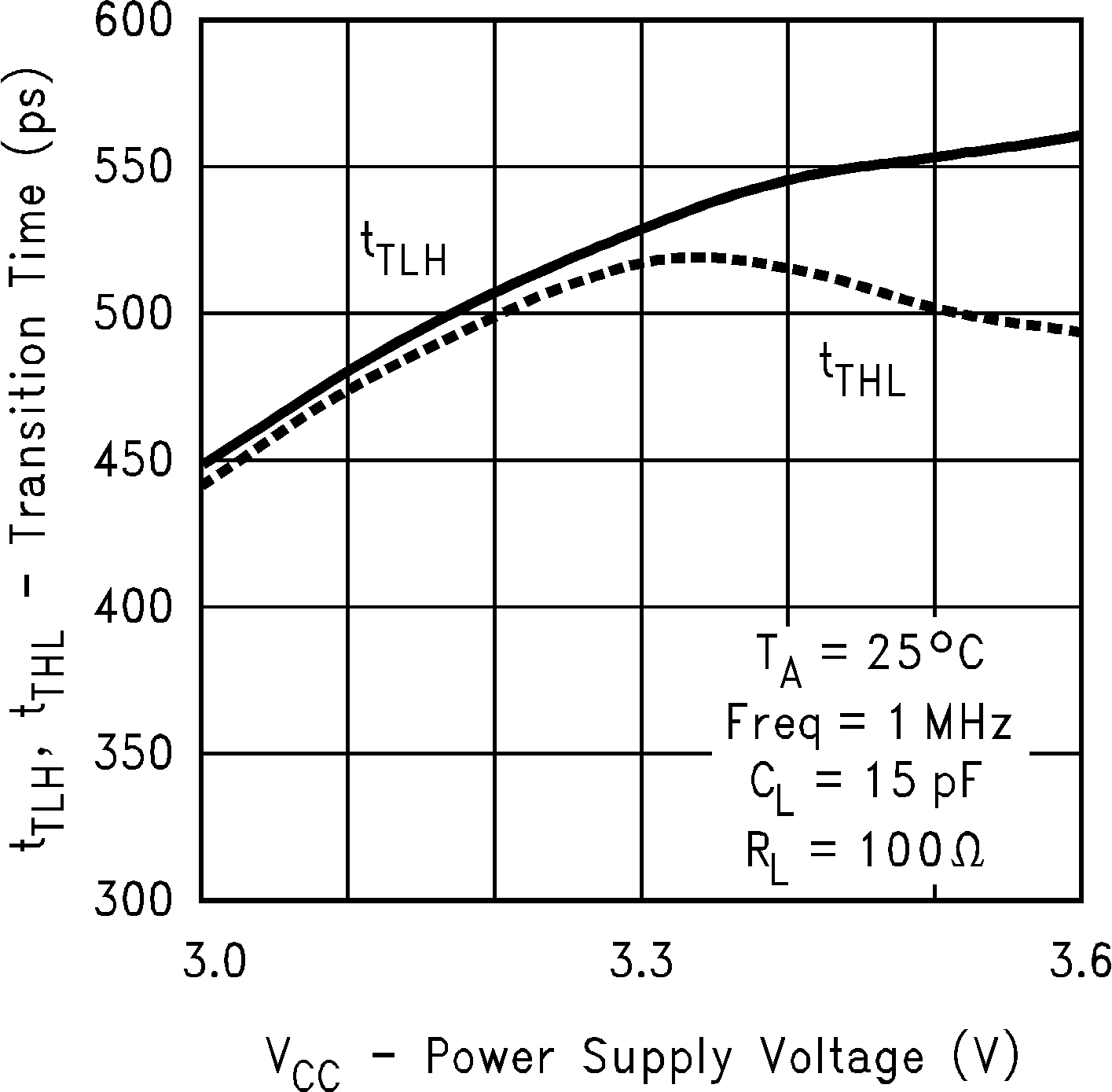 Figure 14. Transition Time vs Power Supply Voltage
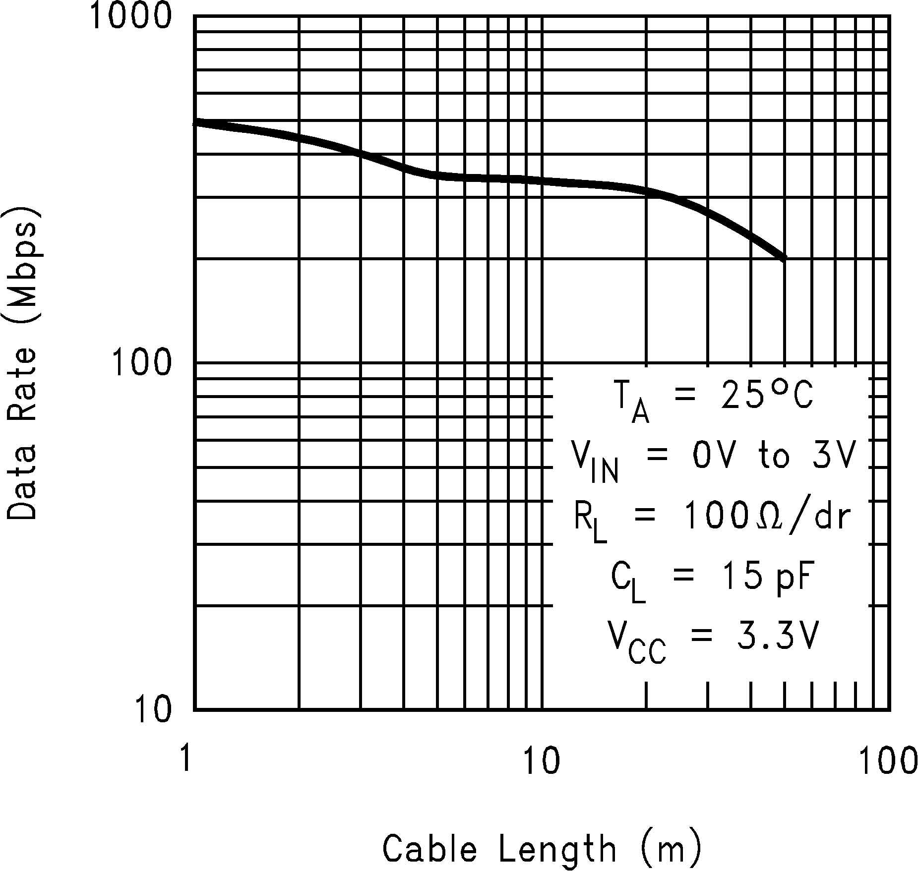 Figure 16. Data Rate vs Cable Length
7 Parameter Measurement Information
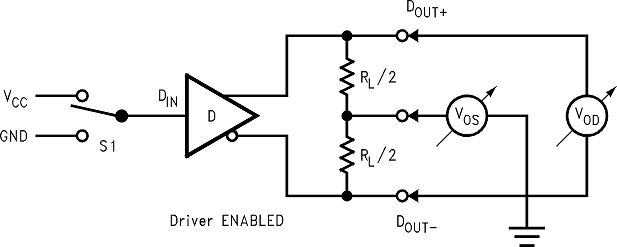 Figure 17. Driver VOD and VOS Test Circuit
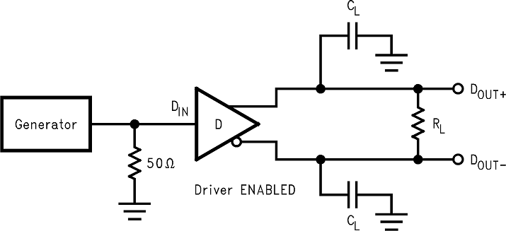 Figure 18. Driver Propagation Delay and Transition Time Test Circuit
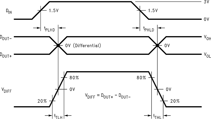 Figure 19. Driver Propagation Delay and Transition Time Waveforms
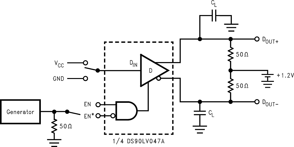 Figure 20. Driver TRI-STATE Delay Test Circuit
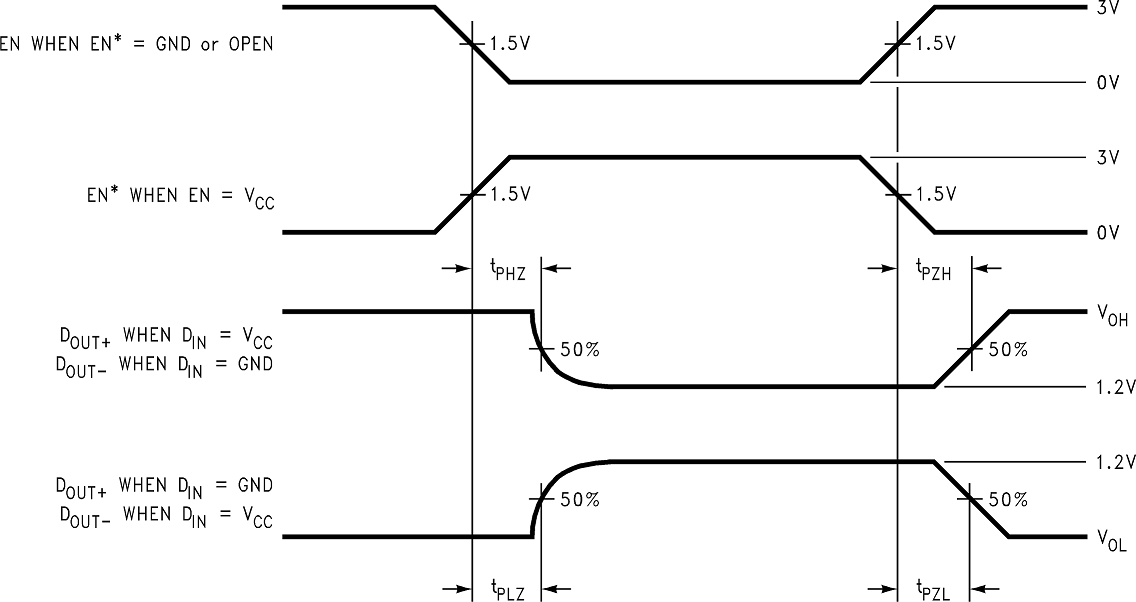 Figure 21. Driver TRI-STATE Delay Waveform
8 Detailed Description
8.1 Overview
LVDS drivers and receivers are intended to be primarily used in an uncomplicated point-to-point configuration as is shown in Figure 23. This configuration provides a clean signaling environment for the fast edge rates of the drivers. The receiver is connected to the driver through a balanced media which may be a standard twisted pair cable, a parallel pair cable, or simply PCB traces. Typically, the characteristic differential impedance of the media is in the range of 100 Ω. A termination resistor of 100 Ω (selected to match the media), and is located as close to the receiver input pins as possible. The termination resistor converts the driver output current (current mode) into a voltage that is detected by the receiver. Other configurations are possible such as a multi-receiver configuration, but the effects of a mid-stream connector(s), cable stub(s), and other impedance discontinuities as well as ground shifting, noise margin limits, and total termination loading must be taken into account.
The DS90LV047A differential line driver is a balanced current source design. A current mode driver, generally speaking has a high output impedance and supplies a constant current for a range of loads (a voltage mode driver on the other hand supplies a constant voltage for a range of loads). Current is switched through the load in one direction to produce a logic state and in the other direction to produce the other logic state. The output current is typically 3.1 mA, a minimum of 2.5 mA, and a maximum of 4.5 mA. The current mode driver requires (as discussed above) that a resistive termination be employed to terminate the signal and to complete the loop as shown in Figure 23. AC or unterminated configurations are not allowed. The 3.1-mA loop current develops a differential voltage of 310 mV across the 100-Ω termination resistor which the receiver detects with a 250-mV minimum differential noise margin, (driven signal minus receiver threshold (250 mV – 100 mV = 150 mV). The signal is centered around +1.2 V (Driver Offset, VOS) with respect to ground as shown in Figure 22.
NOTE
The steady-state voltage (VSS) peak-to-peak swing is twice the differential voltage (VOD) and is typically 620 mV.
The current mode driver provides substantial benefits over voltage mode drivers, such as an RS-422 driver. Its quiescent current remains relatively flat versus switching frequency. Whereas the RS-422 voltage mode driver increases exponentially in most case from 20 MHz to 50 MHz. This is due to the overlap current that flows between the rails of the device when the internal gates switch. Whereas the current mode driver switches a fixed current between its output without any substantial overlap current. This is similar to some ECL and PECL devices, but without the heavy static ICC requirements of the ECL/PECL designs. LVDS requires > 80% less current than similar PECL devices. AC specifications for the driver are a tenfold improvement over other existing RS-422 drivers.
The TRI-STATE function allows the driver outputs to be disabled, thus obtaining an even lower power state when the transmission of data is not required.
8.2 Functional Block Diagram

8.3 Feature Description
8.3.1 LVDS Fail-Safe
This section addresses the common concern of fail-safe biasing of LVDS interconnects, specifically looking at the DS90LV047A driver outputs and the DS90LV048A receiver inputs.
The LVDS receiver is a high-gain, high-speed device that amplifies a small differential signal (20 mV) to CMOS logic levels. Due to the high gain and tight threshold of the receiver, take care to prevent noise from appearing as a valid signal.
The internal fail-safe circuitry of the receiver is designed to source or sink a small amount of current, providing fail-safe protection (a stable known state of HIGH output voltage) for floating, terminated, or shorted receiver inputs.
- Open Input Pins. The DS90LV048A is a quad receiver device, and if an application requires only 1, 2, or 3 receivers, the unused channel(s) inputs must be left OPEN. Do not tie unused receiver inputs to ground or any other voltages. The input is biased by internal high value pullup and pulldown resistors to set the output to a HIGH state. This internal circuitry ensures a HIGH, stable output state for open inputs.
- Terminated Input. If the DS90LV047A driver is disconnected (cable unplugged), or if the DS90LV047A driver is in a TRI-STATE or power-off condition, the receiver output is again in a HIGH state, even with the end of cable 100-Ω termination resistor across the input pins. The unplugged cable can become a floating antenna which can pick up noise. If the cable picks up more than 10 mV of differential noise, the receiver may see the noise as a valid signal and switch. To insure that any noise is seen as common-mode and not differential, a balanced interconnect must be used. Twisted pair cable offers better balance than flat ribbon cable.
- Shorted Inputs. If a fault condition occurs that shorts the receiver inputs together, thus resulting in a 0-V differential input voltage, the receiver output remains in a HIGH state. Shorted input fail-safe is not supported across the common-mode range of the device (GND to 2.4 V). It is only supported with inputs shorted and no external common-mode voltage applied.
External lower value pullup and pulldown resistors (for a stronger bias) may be used to boost fail-safe in the presence of higher noise levels. The pullup and pulldown resistors should be in the 5-kΩ to 15-kΩ range to minimize loading and waveform distortion to the driver. The common-mode bias point should be set to approximately 1.2 V (less than 1.75 V) to be compatible with the internal circuitry.
 Figure 22. Driver Output Levels
8.4 Device Functional Modes
Table 1 lists the functional modes DS90LV047A.
Table 1. Truth Table
| ENABLES | INPUT | OUTPUTS | ||
|---|---|---|---|---|
| EN | EN* | DIN | DOUT+ | DOUT− |
| H | L or Open | L | L | H |
| H | H | L | ||
| All other combinations of ENABLE inputs | X | Z | Z | |