DLPS039G December 2015 – July 2024 TPS99000-Q1
PRODUCTION DATA
- 1
- 1 Features
- 2 Applications
- 3 Description
- 4 Pin Configuration and Functions
-
5 Specifications
- 5.1 Absolute Maximum Ratings
- 5.2 ESD Ratings
- 5.3 Recommended Operating Conditions
- 5.4 Thermal Information
- 5.5 Electrical Characteristics—Transimpedance Amplifier Parameters
- 5.6 Electrical Characteristics—Digital to Analog Converters
- 5.7 Electrical Characteristics—Analog to Digital Converter
- 5.8 Electrical Characteristics—FET Gate Drivers
- 5.9 Electrical Characteristics—Photo Comparator
- 5.10 Electrical Characteristics—Voltage Regulators
- 5.11 Electrical Characteristics—Temperature and Voltage Monitors
- 5.12 Electrical Characteristics—Current Consumption
- 5.13 Power-Up Timing Requirements
- 5.14 Power-Down Timing Requirements
- 5.15 Timing Requirements—Sequencer Clock
- 5.16 Timing Requirements—Host and Diagnostic Port SPI Interface
- 5.17 Timing Requirements—ADC Interface
- 5.18 Switching Characteristics
-
6 Detailed Description
- 6.1 Overview
- 6.2 Functional Block Diagram
- 6.3
Feature Description
- 6.3.1
Illumination Control
- 6.3.1.1 Illumination System High Dynamic Range Dimming Overview
- 6.3.1.2 Illumination Control Loop
- 6.3.1.3 Continuous Mode Operation
- 6.3.1.4
Discontinuous Mode Operation
- 6.3.1.4.1 Discontinuous Mode Pulse Width Limit
- 6.3.1.4.2 COMPOUT_LOW Timer in Discontinuous Operation
- 6.3.1.4.3 Dimming Within Discontinuous Operation Range
- 6.3.1.4.4 Multiple Pulse Heights to Increase Bit Depth
- 6.3.1.4.5 TIA Gain Adjustment
- 6.3.1.4.6 Current Limit in Discontinuous Mode
- 6.3.1.4.7 CMODE Big Cap Mode in Discontinuous Operation
- 6.3.2 Over-Brightness Detection
- 6.3.3 Analog to Digital Converter
- 6.3.4 Power Sequencing and Monitoring
- 6.3.5 DMD Mirror Voltage Regulator
- 6.3.6 Low Dropout Regulators
- 6.3.7 System Monitoring Features
- 6.3.8 Communication Ports
- 6.3.1
Illumination Control
- 6.4 Device Functional Modes
- 6.5 Register Maps
- 7 Application and Implementation
- 8 Power Supply Recommendations
- 9 Layout
- 10Device and Documentation Support
- 11Revision History
- 12Mechanical, Packaging, and Orderable Information
6.3.1.4.7 CMODE Big Cap Mode in Discontinuous Operation
The TPS99000-Q1 provides an output signal, CMODE, that can be used to drive the gate of a FET that switches in a larger capacitor for discontinuous operation. High-capacitance mode is only used during discontinuous operation. (High capacitance causes issues in continuous operation, minimizing capacitance is preferred for that mode). The higher capacitance slows the rate at which the forward voltage of the LED increases during the pulse creation process. The slower charge rate causes the transition from no light emission to full light emission to extend in time. In selecting the proper capacitance, a balance between good edge rate control and the total time for the pulse to reach the threshold must be made. Attention should be paid to the temperature characteristics of this capacitor. Less variation of capacitance over temperature will result in more accurate, repeatable results in cold/hot conditions.
Benefits:
- Pulse stability
- Support for lower light output thresholds, due to slower pulse edge rates
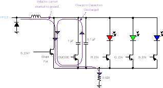
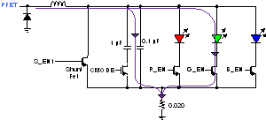
The charge and discharge loops using the CMODE big cap are as follows:
 Figure 6-24 Discontinuous Mode Current Paths with Shunt Enabled
 Figure 6-25 Discontinuous Mode Current Paths with Shunt Disabled