DLPS039G December 2015 – July 2024 TPS99000-Q1
PRODUCTION DATA
- 1
- 1 Features
- 2 Applications
- 3 Description
- 4 Pin Configuration and Functions
-
5 Specifications
- 5.1 Absolute Maximum Ratings
- 5.2 ESD Ratings
- 5.3 Recommended Operating Conditions
- 5.4 Thermal Information
- 5.5 Electrical Characteristics—Transimpedance Amplifier Parameters
- 5.6 Electrical Characteristics—Digital to Analog Converters
- 5.7 Electrical Characteristics—Analog to Digital Converter
- 5.8 Electrical Characteristics—FET Gate Drivers
- 5.9 Electrical Characteristics—Photo Comparator
- 5.10 Electrical Characteristics—Voltage Regulators
- 5.11 Electrical Characteristics—Temperature and Voltage Monitors
- 5.12 Electrical Characteristics—Current Consumption
- 5.13 Power-Up Timing Requirements
- 5.14 Power-Down Timing Requirements
- 5.15 Timing Requirements—Sequencer Clock
- 5.16 Timing Requirements—Host and Diagnostic Port SPI Interface
- 5.17 Timing Requirements—ADC Interface
- 5.18 Switching Characteristics
-
6 Detailed Description
- 6.1 Overview
- 6.2 Functional Block Diagram
- 6.3
Feature Description
- 6.3.1
Illumination Control
- 6.3.1.1 Illumination System High Dynamic Range Dimming Overview
- 6.3.1.2 Illumination Control Loop
- 6.3.1.3 Continuous Mode Operation
- 6.3.1.4
Discontinuous Mode Operation
- 6.3.1.4.1 Discontinuous Mode Pulse Width Limit
- 6.3.1.4.2 COMPOUT_LOW Timer in Discontinuous Operation
- 6.3.1.4.3 Dimming Within Discontinuous Operation Range
- 6.3.1.4.4 Multiple Pulse Heights to Increase Bit Depth
- 6.3.1.4.5 TIA Gain Adjustment
- 6.3.1.4.6 Current Limit in Discontinuous Mode
- 6.3.1.4.7 CMODE Big Cap Mode in Discontinuous Operation
- 6.3.2 Over-Brightness Detection
- 6.3.3 Analog to Digital Converter
- 6.3.4 Power Sequencing and Monitoring
- 6.3.5 DMD Mirror Voltage Regulator
- 6.3.6 Low Dropout Regulators
- 6.3.7 System Monitoring Features
- 6.3.8 Communication Ports
- 6.3.1
Illumination Control
- 6.4 Device Functional Modes
- 6.5 Register Maps
- 7 Application and Implementation
- 8 Power Supply Recommendations
- 9 Layout
- 10Device and Documentation Support
- 11Revision History
- 12Mechanical, Packaging, and Orderable Information
6.3.1.4.3 Dimming Within Discontinuous Operation Range
When operating in discontinuous mode, two methods of dimming are used concurrently to reduce the brightness of the display:
- Amplitude dimming using the photo feedback DAC settings.
- Controlling the number of pulses per bit slice (via commands to DLPC23x-Q1, selecting specific lookup table data).
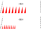
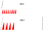
Figure 6-20 is an example of the brightest LUT data table having 8 pulses per LSB (smallest bit slice). The LED pulse height is modulated to achieve a 2:1 dimming ratio while still maintaining 8 pulses per LSB. To allow for a seamless transition to lower dimming levels, a change to 4 pulses per LSB plus higher LED amplitude is made as illustrated in Figure 6-21. The total light generated in both cases in Figure 6-21 is approximately equal. A system calibration is used to determine this ½ LED amplitude photo feedback DAC setting.
 Figure 6-20 2:1 Dimming Within a Sequence
 Figure 6-21 Discontinuous Operation Pulse Count Change
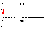
As a smooth dimming (brightness going down) sequence continues, the process above eventually results in using 1 pulse per LSB. Amplitude dimming is used to dim to the absolute minimum display brightness level as illustrated in Figure 6-22.
 Figure 6-22 Discontinuous Dimming with One Pulse Per LSB Sequence
As shown in Figure 6-22, once a single pulse-per-LSB is selected, all remaining dimming must occur using only pulse height threshold reduction.