DLPU040C October   2016  – July 2024 DLP650LNIR , DLPC410


  1.   1
  2.   Description
  3.   Features
  4.   4
  5. 1Evaluation Module Overview
    1. 1.1 Introduction
    2. 1.2 Overview
      1. 1.2.1 The DLP Discovery 4100 Development Platform
      2. 1.2.2 DLP Discovery 4100 Development Platform Photo
  6. 2Hardware
    1. 2.1 Key Components
      1. 2.1.1  Xilinx Virtex 5 APPSFPGA
      2. 2.1.2  DLPC410 - Digital Controller for DLP Discovery 4100 Chipset
      3. 2.1.3  DLPA200 - DMD Micromirror Driver
      4. 2.1.4  DLPR410 - Configuration PROM for DLPC410 Controller
      5. 2.1.5  APPSFPGA Flash Configuration PROM
      6. 2.1.6  DMD Connectors
      7. 2.1.7  USB Controller
      8. 2.1.8  50MHz Oscillator
      9. 2.1.9  DDR2 SODIMM Connector
      10. 2.1.10 Connectors
        1. 2.1.10.1 JTAG Header H1
        2. 2.1.10.2 Mictor Connectors
        3. 2.1.10.3 GPIO Connectors
      11. 2.1.11 Battery
      12. 2.1.12 Power Supplies
        1. 2.1.12.1 J12 Power Connector
        2. 2.1.12.2 J18 Power Connector
        3. 2.1.12.3 REG. 0.9V
        4. 2.1.12.4 REG. 1.0V
        5. 2.1.12.5 REG. 1.8V
        6. 2.1.12.6 REG. 2.5V
        7. 2.1.12.7 REG. 3.3V
        8. 2.1.12.8 REG. 12V
    2. 2.2 Hardware Overview and Setup
      1. 2.2.1 Getting Started
      2. 2.2.2 User Connectors and I/O
        1. 2.2.2.1  J12 Input Power Connector
        2. 2.2.2.2  J18 Input Power Connector
        3. 2.2.2.3  J1 USB Connector Pinout
        4. 2.2.2.4  J3 USB GPIO
        5. 2.2.2.5  J6 GPIO_A Connector
        6. 2.2.2.6  J8 DLPC410 Mictor Connector
        7. 2.2.2.7  J9 USB/APPSFPGA Mictor Connector
        8. 2.2.2.8  J13 DMD Flex 1 Connector
        9. 2.2.2.9  J14 DMD Flex 2 Connector
        10. 2.2.2.10 J15 - DDR2 SODIMM Connector
        11. 2.2.2.11 J16, J17 EXP Connectors
        12. 2.2.2.12 H1 Xilinx FPGA JTAG Header
      3. 2.2.3 Configuration Jumpers
        1. 2.2.3.1 J2 – EXP Voltage Select
        2. 2.2.3.2 J4 – APPSFPGA Revision Select
        3. 2.2.3.3 J5 – Shared USB Signal Enable/Disable
        4. 2.2.3.4 J7 – USB EEPROM Programming Header
        5. 2.2.3.5 J10 – DLPA200 B Output Enable
      4. 2.2.4 Switches
        1. 2.2.4.1 SW1 - APPSFPGA Functional Switches
        2. 2.2.4.2 SW2 - APPSFPGA Reset
        3. 2.2.4.3 SW3 - DMD Power Float (Park)
        4. 2.2.4.4 SW4 - Input Power On/Off
      5. 2.2.5 Power and Status LEDs
        1. 2.2.5.1 D1 – USB Connection Indicator
        2. 2.2.5.2 D2 and D16 – APPSFPGA Done
        3. 2.2.5.3 D3 and D17 – DLPC410 Done
        4. 2.2.5.4 D9 – DDC_LED0
        5. 2.2.5.5 D10 – DDC_LED1
        6. 2.2.5.6 D11 – VLED0
        7. 2.2.5.7 D12 – VLED1
      6. 2.2.6 Test Points
  7. 3Software
    1. 3.1 Overview
      1. 3.1.1 Software Overview
        1. 3.1.1.1 DMD Image Control
        2. 3.1.1.2 Image Commands
    2. 3.2 DLP Discovery 4100 Operation
      1. 3.2.1 Quick Start Guide on Operation
    3. 3.3 Graphical User Interface
      1. 3.3.1 Menu Bar
        1. 3.3.1.1 File Menu
        2. 3.3.1.2 View Menu
        3. 3.3.1.3 DMD Menu
        4. 3.3.1.4 Execution Menu
        5. 3.3.1.5 Test Patterns Menu
        6. 3.3.1.6 Help Menu
      2. 3.3.2 Toolbar
        1. 3.3.2.1 File Menu Buttons
        2. 3.3.2.2 Run, Run Once, Loop Break, Step and Stop Controls
        3. 3.3.2.3 Set Start and End Buttons
        4. 3.3.2.4 Help Button
      3. 3.3.3 Script Commands Window
        1. 3.3.3.1 Load Tab
        2. 3.3.3.2 Reset Tab
        3. 3.3.3.3 Clear Tab
        4. 3.3.3.4 Float Tab
        5. 3.3.3.5 Control Tab
      4. 3.3.4 Status Window
      5. 3.3.5 Script Window
        1. 3.3.5.1 Inserting Commands
        2. 3.3.5.2 Moving Commands
        3. 3.3.5.3 Deleting Commands
    4. 3.4 Script and Status Operations
      1. 3.4.1 Saving Scripts and Statuses
        1. 3.4.1.1 Saving a Script
        2. 3.4.1.2 Saving a Status
      2. 3.4.2 Printing Scripts and Statuses
        1. 3.4.2.1 Printing a Script
        2. 3.4.2.2 Printing a Status
      3. 3.4.3 Opening Scripts and Statuses
      4. 3.4.4 Creating New Scripts and Statuses
        1. 3.4.4.1 Creating a New Script
        2. 3.4.4.2 Creating a New Status
    5. 3.5 DLPC410 Control Window
    6. 3.6 Test Patterns Window
    7. 3.7 About Box
    8. 3.8 Links
  8. 4Hardware Design Files
  9. 5Additional Information
    1. 5.1 Trademarks
    2. 5.2 Abbreviations and Acronyms
    3. 5.3 Notational Conventions
      1. 5.3.1 Information About Cautions and Warnings
  10. 6Related Documentation
  11. 7Revision History

DLPC410 Control Window

The DLPC410 Control window is accessed through the DMD/DLPC410 Control menu and provides direct control of the DLPC410 input signals. No script commands are generated, the control is applied immediately to the DLPC410 when a Set button is clicked.

The upper portion of the window supports reading and setting of the DLPC410 signals used in writing data to the DMD. The current value for ROWMD (Row Mode), ROWADDR (Row Address), BLKMD (Block Mode), and BLKADDR (Block Address) is displayed in the Current Value column. When a new value is entered in Hexadecimal in the Hex column and the Set button is clicked the value sent to the DLPC410. The Load Row button sends one row with repeating values of the 4 digit hex value entered.

The lower portion of the window supports control of the DLPC410 input signals which are control operational modes. Click a button to toggle the current value of the signal.

Note: Asserting PWRFLOAT (Power Float) Parks the DMD mirrors. Recovery requires reset to the APPSFPGA either via asserting APPS_LOGIC_RST (HW switch SW2) or power cycling the EVM to restart the operation of the D4100 system again.

Refer to the DLPC410 data sheet (DLPS024) for detailed information on the DLPC410 input signals.

Refer to the DLP Discovery 4100 Development Platform API Programmer’s Guide (DLPU039) for detailed information about the ActiveX functions called by the buttons on this DMD/DLPC410 Control menu page.
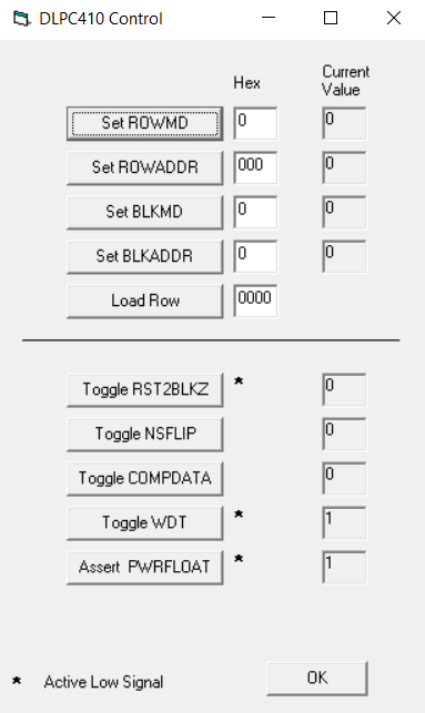
DLPLCRC410EVM, DLPLCR65NEVM, DLPLCR70EVM, DLPLCR70UVEVM, DLPLCR95EVM, DLPLCR95UVEVM DLPC410 Control WindowFigure 3-29 DLPC410 Control Window