DLPU040C October   2016  – July 2024 DLP650LNIR , DLPC410


  1.   1
  2.   Description
  3.   Features
  4.   4
  5. 1Evaluation Module Overview
    1. 1.1 Introduction
    2. 1.2 Overview
      1. 1.2.1 The DLP Discovery 4100 Development Platform
      2. 1.2.2 DLP Discovery 4100 Development Platform Photo
  6. 2Hardware
    1. 2.1 Key Components
      1. 2.1.1  Xilinx Virtex 5 APPSFPGA
      2. 2.1.2  DLPC410 - Digital Controller for DLP Discovery 4100 Chipset
      3. 2.1.3  DLPA200 - DMD Micromirror Driver
      4. 2.1.4  DLPR410 - Configuration PROM for DLPC410 Controller
      5. 2.1.5  APPSFPGA Flash Configuration PROM
      6. 2.1.6  DMD Connectors
      7. 2.1.7  USB Controller
      8. 2.1.8  50MHz Oscillator
      9. 2.1.9  DDR2 SODIMM Connector
      10. 2.1.10 Connectors
        1. 2.1.10.1 JTAG Header H1
        2. 2.1.10.2 Mictor Connectors
        3. 2.1.10.3 GPIO Connectors
      11. 2.1.11 Battery
      12. 2.1.12 Power Supplies
        1. 2.1.12.1 J12 Power Connector
        2. 2.1.12.2 J18 Power Connector
        3. 2.1.12.3 REG. 0.9V
        4. 2.1.12.4 REG. 1.0V
        5. 2.1.12.5 REG. 1.8V
        6. 2.1.12.6 REG. 2.5V
        7. 2.1.12.7 REG. 3.3V
        8. 2.1.12.8 REG. 12V
    2. 2.2 Hardware Overview and Setup
      1. 2.2.1 Getting Started
      2. 2.2.2 User Connectors and I/O
        1. 2.2.2.1  J12 Input Power Connector
        2. 2.2.2.2  J18 Input Power Connector
        3. 2.2.2.3  J1 USB Connector Pinout
        4. 2.2.2.4  J3 USB GPIO
        5. 2.2.2.5  J6 GPIO_A Connector
        6. 2.2.2.6  J8 DLPC410 Mictor Connector
        7. 2.2.2.7  J9 USB/APPSFPGA Mictor Connector
        8. 2.2.2.8  J13 DMD Flex 1 Connector
        9. 2.2.2.9  J14 DMD Flex 2 Connector
        10. 2.2.2.10 J15 - DDR2 SODIMM Connector
        11. 2.2.2.11 J16, J17 EXP Connectors
        12. 2.2.2.12 H1 Xilinx FPGA JTAG Header
      3. 2.2.3 Configuration Jumpers
        1. 2.2.3.1 J2 – EXP Voltage Select
        2. 2.2.3.2 J4 – APPSFPGA Revision Select
        3. 2.2.3.3 J5 – Shared USB Signal Enable/Disable
        4. 2.2.3.4 J7 – USB EEPROM Programming Header
        5. 2.2.3.5 J10 – DLPA200 B Output Enable
      4. 2.2.4 Switches
        1. 2.2.4.1 SW1 - APPSFPGA Functional Switches
        2. 2.2.4.2 SW2 - APPSFPGA Reset
        3. 2.2.4.3 SW3 - DMD Power Float (Park)
        4. 2.2.4.4 SW4 - Input Power On/Off
      5. 2.2.5 Power and Status LEDs
        1. 2.2.5.1 D1 – USB Connection Indicator
        2. 2.2.5.2 D2 and D16 – APPSFPGA Done
        3. 2.2.5.3 D3 and D17 – DLPC410 Done
        4. 2.2.5.4 D9 – DDC_LED0
        5. 2.2.5.5 D10 – DDC_LED1
        6. 2.2.5.6 D11 – VLED0
        7. 2.2.5.7 D12 – VLED1
      6. 2.2.6 Test Points
  7. 3Software
    1. 3.1 Overview
      1. 3.1.1 Software Overview
        1. 3.1.1.1 DMD Image Control
        2. 3.1.1.2 Image Commands
    2. 3.2 DLP Discovery 4100 Operation
      1. 3.2.1 Quick Start Guide on Operation
    3. 3.3 Graphical User Interface
      1. 3.3.1 Menu Bar
        1. 3.3.1.1 File Menu
        2. 3.3.1.2 View Menu
        3. 3.3.1.3 DMD Menu
        4. 3.3.1.4 Execution Menu
        5. 3.3.1.5 Test Patterns Menu
        6. 3.3.1.6 Help Menu
      2. 3.3.2 Toolbar
        1. 3.3.2.1 File Menu Buttons
        2. 3.3.2.2 Run, Run Once, Loop Break, Step and Stop Controls
        3. 3.3.2.3 Set Start and End Buttons
        4. 3.3.2.4 Help Button
      3. 3.3.3 Script Commands Window
        1. 3.3.3.1 Load Tab
        2. 3.3.3.2 Reset Tab
        3. 3.3.3.3 Clear Tab
        4. 3.3.3.4 Float Tab
        5. 3.3.3.5 Control Tab
      4. 3.3.4 Status Window
      5. 3.3.5 Script Window
        1. 3.3.5.1 Inserting Commands
        2. 3.3.5.2 Moving Commands
        3. 3.3.5.3 Deleting Commands
    4. 3.4 Script and Status Operations
      1. 3.4.1 Saving Scripts and Statuses
        1. 3.4.1.1 Saving a Script
        2. 3.4.1.2 Saving a Status
      2. 3.4.2 Printing Scripts and Statuses
        1. 3.4.2.1 Printing a Script
        2. 3.4.2.2 Printing a Status
      3. 3.4.3 Opening Scripts and Statuses
      4. 3.4.4 Creating New Scripts and Statuses
        1. 3.4.4.1 Creating a New Script
        2. 3.4.4.2 Creating a New Status
    5. 3.5 DLPC410 Control Window
    6. 3.6 Test Patterns Window
    7. 3.7 About Box
    8. 3.8 Links
  8. 4Hardware Design Files
  9. 5Additional Information
    1. 5.1 Trademarks
    2. 5.2 Abbreviations and Acronyms
    3. 5.3 Notational Conventions
      1. 5.3.1 Information About Cautions and Warnings
  10. 6Related Documentation
  11. 7Revision History

Control Tab

The Control commands tab supports commands for script execution control, external reset, and digital output:

  • The Wait for External Reset scripting command waits 10 seconds for an external global reset triggered by a rising edge on APPSFPGA input GPIO_A0. After 10 seconds, execution of the script resumes with the next command in the script. GPIO_A0 is a 2.5 Volt CMOS input.
  • The Delay command delays for the specified time in msec.
  • The Loop Until Break command loops until the Break button is clicked.
  • The Loop command loops for the specified number of iterations.
  • The Set GP Output command sets the value of the APPSFPGA general purpose digital outputs GPIO_A(4 - 6). Value is entered in decimal or hexadecimal (for example, 0x3). Bits 0, 1, 2 of value control the output state of GPIO_A4, GPIO_A5, and GPIO_A6 respectively. Bits 7, 6, 5, 4, 3 of Value are not used. GPIO_A(4 - 6) are 2.5 Volt CMOS outputs.
    Note: NOTE: For more information on GPIO outputs see the DLP® Discovery™ 4100 Development Platform API Programmer’s Guide (DLPU039 § 5.2.24 and § 6.2.24).
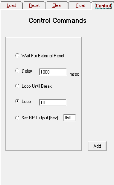
DLPLCRC410EVM, DLPLCR65NEVM, DLPLCR70EVM, DLPLCR70UVEVM, DLPLCR95EVM, DLPLCR95UVEVM Control TabFigure 3-26 Control Tab