DLPU040C October 2016 – July 2024 DLP650LNIR , DLPC410
- 1
- Description
- Features
- 4
- 1Evaluation Module Overview
-
2Hardware
- 2.1
Key Components
- 2.1.1 Xilinx Virtex 5 APPSFPGA
- 2.1.2 DLPC410 - Digital Controller for DLP Discovery 4100 Chipset
- 2.1.3 DLPA200 - DMD Micromirror Driver
- 2.1.4 DLPR410 - Configuration PROM for DLPC410 Controller
- 2.1.5 APPSFPGA Flash Configuration PROM
- 2.1.6 DMD Connectors
- 2.1.7 USB Controller
- 2.1.8 50MHz Oscillator
- 2.1.9 DDR2 SODIMM Connector
- 2.1.10 Connectors
- 2.1.11 Battery
- 2.1.12 Power Supplies
- 2.2
Hardware Overview and Setup
- 2.2.1 Getting Started
- 2.2.2
User Connectors and I/O
- 2.2.2.1 J12 Input Power Connector
- 2.2.2.2 J18 Input Power Connector
- 2.2.2.3 J1 USB Connector Pinout
- 2.2.2.4 J3 USB GPIO
- 2.2.2.5 J6 GPIO_A Connector
- 2.2.2.6 J8 DLPC410 Mictor Connector
- 2.2.2.7 J9 USB/APPSFPGA Mictor Connector
- 2.2.2.8 J13 DMD Flex 1 Connector
- 2.2.2.9 J14 DMD Flex 2 Connector
- 2.2.2.10 J15 - DDR2 SODIMM Connector
- 2.2.2.11 J16, J17 EXP Connectors
- 2.2.2.12 H1 Xilinx FPGA JTAG Header
- 2.2.3 Configuration Jumpers
- 2.2.4 Switches
- 2.2.5 Power and Status LEDs
- 2.2.6 Test Points
- 2.1
Key Components
-
3Software
- 3.1 Overview
- 3.2 DLP Discovery 4100 Operation
- 3.3 Graphical User Interface
- 3.4 Script and Status Operations
- 3.5 DLPC410 Control Window
- 3.6 Test Patterns Window
- 3.7 About Box
- 3.8 Links
- 4Hardware Design Files
- 5Additional Information
- 6Related Documentation
- 7Revision History
3.6 Test Patterns Window
The Applications FPGA (APPSFPGA) supports two modes.
- Internal Test Patterns Mode - Fixed test patterns stored in the APPSFPGA are selected and displayed on the DMD. This mode does not support scripting.
- User Pattern Mode - User defined images can be downloaded to the APPSFPGA from the GUI for display on the DMD. This is done using the Script Window. When a script is run, the GUI automatically switches to User Pattern Mode even if Internal Test Patterns Mode was previously enabled.
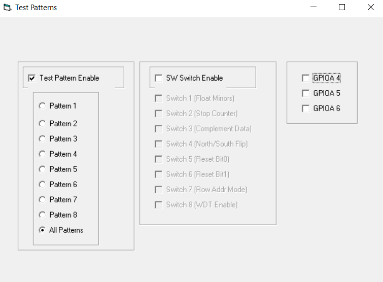
The Test Patterns window is accessed through the Test Patterns menu as seen in Figure 4-30.
 Figure 3-30 Test Patterns Window
The Test Patterns window provides the following functions:
- Enable/Disable Internal Test Patterns Mode. If Internal Test Patterns Mode is enabled, then various internal patterns can be selected to display on the DMD. When "All Patterns" is selected then all internal patterns are displayed in round-robin fashion.
- Enable/Disable Software Switch Override. When enabled, this switch overrides the hardware switch settings of switch SW1 found on the DLPLCRC410EVM Controller Board. The HW DIP Switch assignments are repeated here in Table 4-2 for clarity.
- GPIO_A(4 - 6) enable/disable. The [GPIOA 4], [GPIOA 5], and [GPIOA 6] selections in the Test Patterns window map directly to the GPIO_A4, GPIO_A5, and GPIO_A6 outputs of the APPSFPGA, found on connector GPIO_A.
Table 3-2 SW1 Dip Switch Assignments
| HW Switch SW1 Number | Effect |
|---|---|
| 1 | ON = float – float all mirrors |
| 2 | ON = counter halt – stop counter, this freezes the image on the DMD |
| 3 | ON = complement data – causes DLPC410 to complement all data received |
| 4 | ON = north/south flip – causes the DLPC410 to reverse order of row loading, effectively flipping the image |
| 6 and 5 | Dictates the type of reset being used (where switch 6 is the MSB
and ON = 1):
|
| 7 | ON = Row Address Mode |
| 8 | ON = Watchdog Timer (WDT) Enable, disables other resets |
Refer to the DLP Discovery 4100 Development Platform API Programmer’s Guide (DLPU039) for detailed information about the ActiveX functions called by the buttons on this Test Patterns menu page.