DLPU106A March 2021 – October 2021 DLP3021-Q1
5.1.6 Flash Blocks
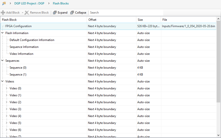
The flash memory for the DGP system is divided into five major blocks. Creation of the flash binary is handled entirely by DLP Composer. The FPGA Configuration for the Xilinx XA7S15-1CPGA196Q Spartan®-7 FPGA is already compiled and included with the example project provided by Texas Instruments.
 Figure 5-6 DLP Composer - Flash Blocks
|
DATA |
ADDRESS |
LENGTH |
|---|---|---|
|
FPGA Configuration |
0x0 |
0x838DC |
|
Flash Information |
0x83900 |
Variable |
|
Default Configuration (Defconfig) |
Variable |
Variable |
|
Sequence 1 |
Variable |
0x1000 |
|
Sequence 2 |
Variable |
0x1000 |
|
Sequence … |
Variable |
0x1000 |
|
Sequence n |
Variable |
0x1000 |
|
Video / Image 1 |
Variable |
Variable |
|
Video / Image 2 |
Variable |
Variable |
|
Video / Image … |
Variable |
Variable |
|
Video / Image n |
Variable |
Variable |
FPGA Configuration
The FPGA configuration block is always located at address 0x0, and is always a fixed size of 0x838DC bytes. This size is derived from the Xilinx XA7S15 specification for maximum configuration length. See the Xilinx UG470 (https://www.xilinx.com/support/documentation/user_guides/ug470_7Series_Config.pdf) for additional details.
Flash Information
The flash information block provides metadata regarding the contents of the flash. This is intended to allow an external MCU or software tool understand the contents of the flash. For example, it defines the locations of the videos within flash so that they can be loaded dynamically by an MCU, such as the MSP430G2553-Q1 on the EVM. The flash information block is divided into four main sections as shown in Table 5-2. Information such as the number of sequences is provided so that software can navigate the flash block and determine the correct offset for the data of interest. The number of sequence and video entries in the information block is variable, but each entry is a fixed size.
|
Offset (HEX) |
0 |
1 |
2 |
3 |
|---|---|---|---|---|
|
00 |
Major |
Minor |
Patch |
|
|
04 |
“D” |
“E” |
“F” |
“C” |
|
08 |
Block Address |
|||
|
0C |
Count (Number of Register Writes) |
|||
|
10 |
“S” |
“E” |
“Q” |
“L” |
|
14 |
Size (of Sequence Block) |
|||
|
18 |
Count (Number of Sequences) |
|||
|
1C |
Sequence 0 Address |
|||
|
20 |
Seq 0 Red Duty Cycle |
Seq 0 Green Duty Cycle |
||
|
24 |
Seq 0 Blue Duty Cycle |
Seq 0 Frame Rate |
||
|
28 |
Sequence 1 Address |
|||
|
2C |
Seq 1 Red Duty Cycle |
Seq 1 Red Duty Cycle |
||
|
30 |
Seq 1 Blue Duty Cycle |
Seq 1 Blue Duty Cycle |
||
|
34 |
Sequence … Address |
|||
|
38 |
Seq … Red Duty Cycle |
Seq … Red Duty Cycle |
||
|
3C |
Seq … Blue Duty Cycle |
Seq … Blue Duty Cycle |
||
|
Variable |
“V” |
“I” |
“D” |
“E” |
|
Variable |
Size (of Video Block) |
|||
|
Variable |
Count (Number of Videos) |
|||
|
Variable |
Video 0 Address |
|||
|
Variable |
Video 0 Frame Rate |
Video 0 Frame Count |
||
|
Variable |
Video 1 Address |
|||
|
Variable |
Video 1 Frame Rate |
Video 1 Frame Rate |
||
|
Variable |
Video … Address |
|||
|
Variable |
Video … Frame Rate |
Video … Frame Rate |
||
Sequences
Sequences are generated by DLP Composer based on the duty cycle selection. Each sequence entry is reserved 4kB in flash.
Videos
Videos and still image content are an input to a dynamic ground projection project in DLP Composer. Composer takes the content, scales it, converts it to a sequence of DMD native format bit-planes, and compresses it using run length encoding (RLE) for storage in flash. When a video or still image is to be shown, the FPGA decompresses each bit-plane and displays in the order and with the timings specified by the sequence.
Default Configuration
The default configuration block is the set of values for each of the FPGA registers. This information is loaded by the FPGA after the completion of the FPGA configuration. These values supersede the power-on default values described in the DLP3021-Q1 FPGA User’s Guide. Default configuration values can be set using DLP Composer on the Default Register Configuration page.