DLPU133 March 2024 DLPC964
- 1
- Abstract
- Trademarks
- 1Overview
-
2Apps FPGA
Modules
- 3.1 Apps FPGA Block Diagram
- 3.2 BPG Module
- 3.3 BRG Module
- 3.4 BRG_ST Module
- 3.5 PGEN Module
- 3.6 PGEN_MCTRL Module
- 3.7 PGEN_SCTRL Module
- 3.8 PGEN_PRM Module
- 3.9 PGEN_ADDR_ROM
- 3.10 HSSTOP Module
- 3.11 SSF Module
- 3.12 ENC Module
- 3.13 Xilinx IP
- 3.14 Reference Documents
- 3.15 DLPC964 Apps FPGA IO
- 3.16 Key Definitions
- 3Functional Configuration
-
4Appendix
- 5.1 Vivado Chipscope Captures
- 5.2 DLPC964 Apps Bitstream Loading
- 5.3
Interfacing To DLPC964 Controller with Aurora
64B/66B
- 5.3.1 Theory of Operation
- 5.3.2 Overview
- 5.3.3
Aurora 64B/66B TX Core and RTL Generation
- 5.3.3.1 Select Aurora 64B66B From IP Catalog
- 5.3.3.2 Configure Core Options
- 5.3.3.3 Lane Configurations
- 5.3.3.4 Shared Logic Options
- 5.3.3.5 Generate Example Design Files
- 5.3.3.6 RTL File List
- 5.3.3.7 Single Channel 3 Lanes Aurora Core RTL Wrapper
- 5.3.3.8 Four Channels 12 Lanes Top Level RTL Wrapper
- 5.3.3.9 Block Start with Block Control Word
- 5.3.3.10 Block Complete with DMDLOAD_REQ
- 5.3.3.11 DMDLOAD_REQ Setup Time Requirement
- 5.3.3.12 Single Channel Transfer Mode
- 5.3.3.13 DMD Block Array Data Mapping
- 5.3.3.14 Xilinx IBERT
- 5Abbreviations and Acronyms
- 6Related Documentation from Texas Instruments
2.6 PGEN_MCTRL Module
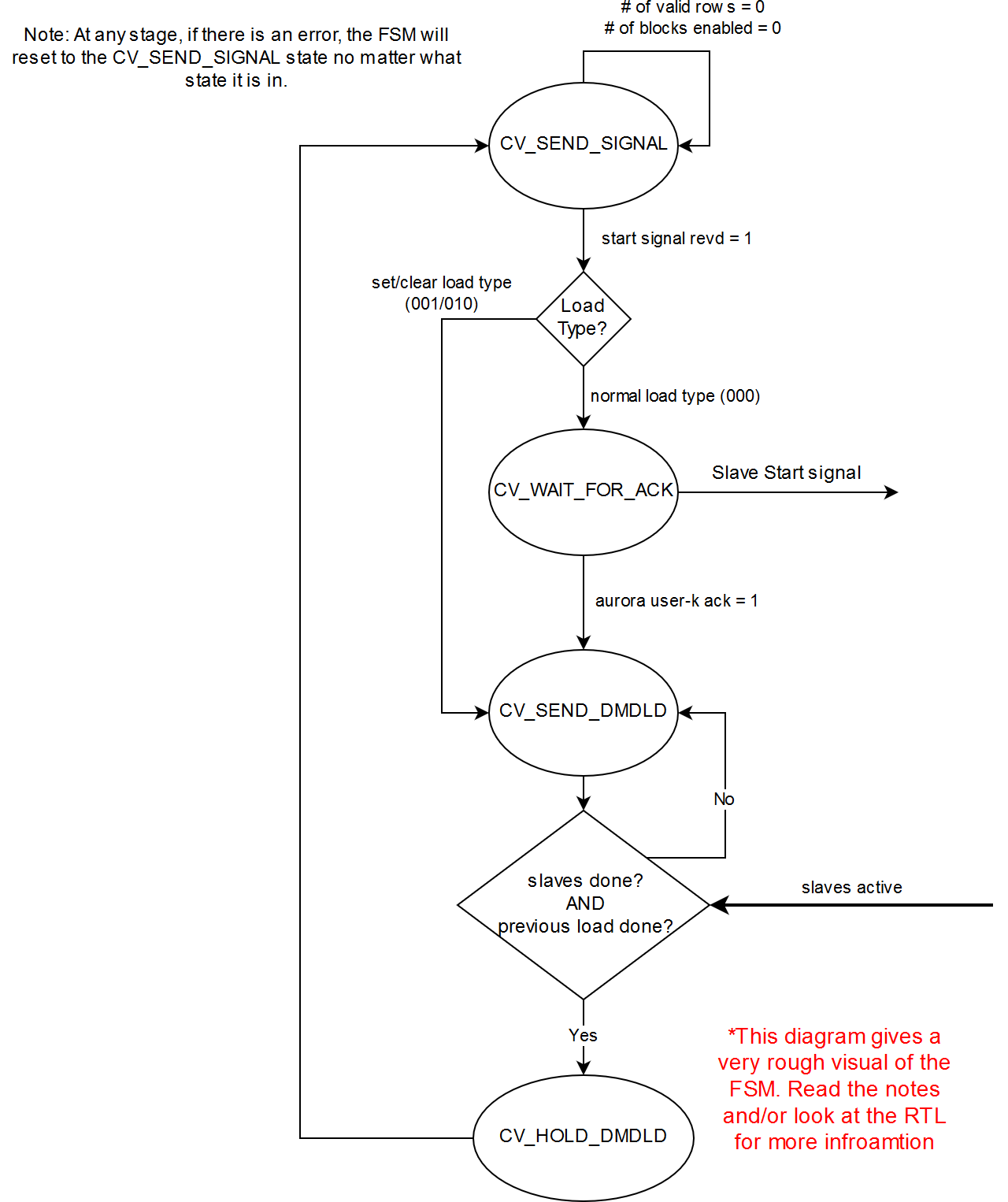
The primary control module is started by the start signal of the BRG, which also controls four copies of the secondary control modules. The secondary control modules are in charge of ROM addressing and outputting biplane images to the DLPC964 controller. The primary control module's core is a Finite State Machine (FSM) that starts off by waiting for the BRG to send the mcp_start signal. Once the signal is sent to the primary module, the FSM initiates. Figure 2-6 depicts the PGEN_MCTRL FSM where each state machine is defined as followed:
- CV_SEND_SIGNAL - Initial FSM state. This transitions states when the BRG start signal is received. Depending on the load type selected, the FSM goes to the CV_WAIT_FOR_ACK state or the CV_SEND_DMDLD state. The command valid signal is not needed when the block load type is Clear (001) or Set (001) because no data is sent during these load types.
- CV_WAIT_FOR_ACK - Once the FSM is started by the BRG, the command valid signal is sent to the Aurora user-k interface. The user-k valid signal is held high in this state until the Aurora user-k ready signal acknowledges the user-k data. Once the FSM is acknowledged, the FSM de-asserts the user-k valid signal and goes to the next FSM state.
- CV_SEND_DMDLD - Now that the command has been sent, the DLPC964 Apps FPGA can start sending bitplane data. This state starts and monitors all four of the secondary control modules. Once all four of the secondary modules report that the modules have completed sending data, the primary control modules can begin to send the DMD load signal over the Aurora user-k interface.
- CV_HOLD_DMDLD - The primary control module holds the DMD load signal until for approximately 0.80ns before transitioning to the beginning of the FSM.
 Figure 2-6 PGEN_MCTRL FSM