DLPU133A March 2024 – February 2025 DLPC964
- 1
- Abstract
- Trademarks
- 1Overview
-
2Apps FPGA
Modules
- 3.1 Apps FPGA Block Diagram
- 3.2 BPG Module
- 3.3 BRG Module
- 3.4 BRG_ST Module
- 3.5 PGEN Module
- 3.6 PGEN_MCTRL Module
- 3.7 PGEN_SCTRL Module
- 3.8 PGEN_PRM Module
- 3.9 PGEN_ADDR_ROM
- 3.10 HSSTOP Module
- 3.11 SSF Module
- 3.12 ENC Module
- 3.13 Xilinx IP
- 3.14 Reference Documents
- 3.15 DLPC964 Apps FPGA IO
- 3.16 Key Definitions
- 3Functional Configuration
-
4Appendix
- 5.1 Vivado Chipscope Captures
- 5.2 DLPC964 Apps Bitstream Loading
- 5.3
Interfacing To DLPC964 Controller with Aurora
64B/66B
- 5.3.1 Theory of Operation
- 5.3.2 Overview
- 5.3.3
Aurora 64B/66B TX Core and RTL Generation
- 5.3.3.1 Select Aurora 64B66B From IP Catalog
- 5.3.3.2 Configure Core Options
- 5.3.3.3 Lane Configurations
- 5.3.3.4 Shared Logic Options
- 5.3.3.5 Generate Example Design Files
- 5.3.3.6 RTL File List
- 5.3.3.7 Single Channel 3 Lanes Aurora Core RTL Wrapper
- 5.3.3.8 Four Channels 12 Lanes Top Level RTL Wrapper
- 5.3.3.9 Block Start with Block Control Word
- 5.3.3.10 Block Complete with DMDLOAD_REQ
- 5.3.3.11 DMDLOAD_REQ Setup Time Requirement
- 5.3.3.12 Single Channel Transfer Mode
- 5.3.3.13 DMD Block Array Data Mapping
- 5.3.3.14 Xilinx IBERT
- 5Abbreviations and Acronyms
- 6Related Documentation from Texas Instruments
- 7Revision History
4.2.2 Loading Bitstream onto Flash
Follow the instructions below for loading the DLPC964 Apps binary onto the flash via a bitstream using Vivado Lab Solutions 2018.2.
Note: Click the link above to download Vivado Lab Solutions
2018.2. Once the webpage is loaded, find the archived 2018.2 folder and then
navigate to the Vivado Lab Solutions 2018.2 downloadable link and download the
installation.
Note: The bitstream is always loaded onto the FPGA upon power-up
of the AMD EVM.
- Plug in the micro USB into the side of the AMD EVM and the other end into the computer running Vivado.
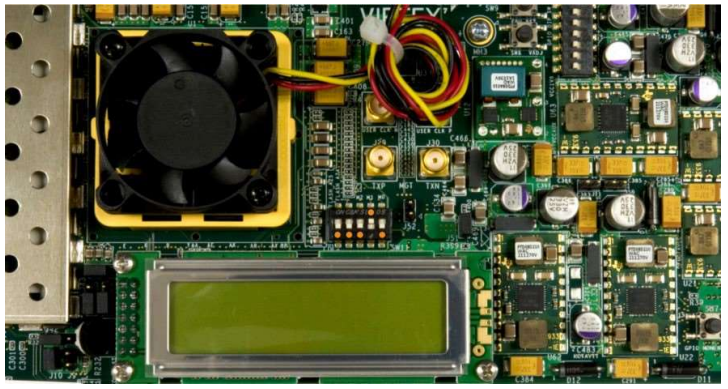
- Make sure to set SW11 to 00010 (1
= on, Position 1 → Position 5, left to right).
 Figure 4-9 FPGA Configuration
Mode
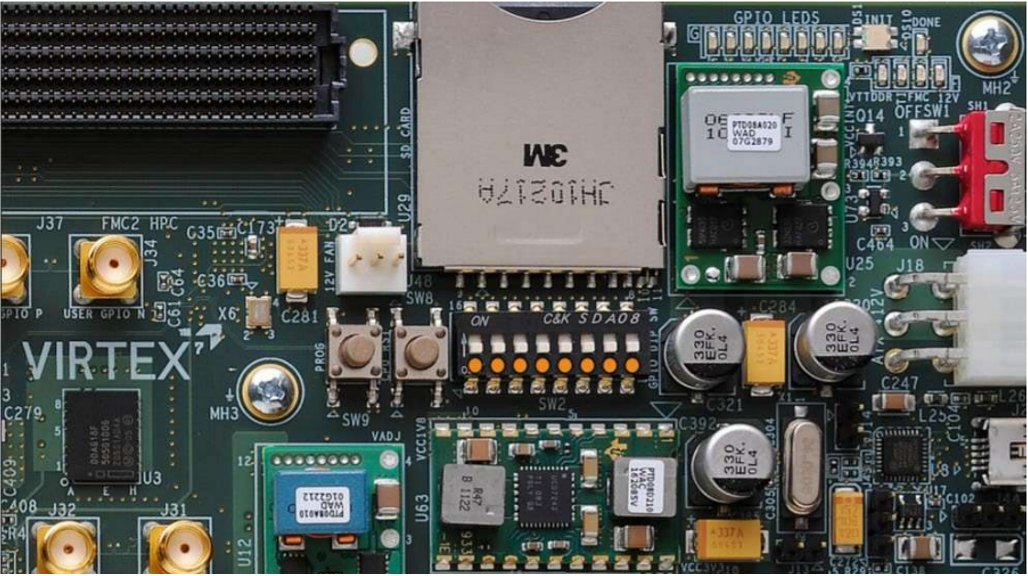
 - Set SW2
to 00000000 (1 = on, Position 1 → Position 8, left to right).
 Figure 4-10 GPIO Dip Switches
(VC707)
 - Start Vivado Lab Studios 2018.2 on the computer.
- Select Open Hardware Manager from the main window.
- Click open target located
in the top left of the hardware manager then Auto Connect.
- If the AMD EVM is the only FPGA plugged into the computer, then Vivado automatically connects to the AMD EVM. Otherwise, the process is slightly more involved.
- Right-click on the FPGA and select Add Configuration Memory Device.
- Find the Flash name mt28gu01gaax1e-bpi-x16 and click OK.
- Select OK again and select
the configuration file (appstop.mcs).
- Make sure all other settings match.
- Once setup, click OK. The programming can take a few minutes.
- Once completed, power cycle the AMD EVM and the DLPC964 Apps Bitstream automatically loads onto the AMD EVM.