DLPU133A March 2024 – February 2025 DLPC964
- 1
- Abstract
- Trademarks
- 1Overview
-
2Apps FPGA
Modules
- 3.1 Apps FPGA Block Diagram
- 3.2 BPG Module
- 3.3 BRG Module
- 3.4 BRG_ST Module
- 3.5 PGEN Module
- 3.6 PGEN_MCTRL Module
- 3.7 PGEN_SCTRL Module
- 3.8 PGEN_PRM Module
- 3.9 PGEN_ADDR_ROM
- 3.10 HSSTOP Module
- 3.11 SSF Module
- 3.12 ENC Module
- 3.13 Xilinx IP
- 3.14 Reference Documents
- 3.15 DLPC964 Apps FPGA IO
- 3.16 Key Definitions
- 3Functional Configuration
-
4Appendix
- 5.1 Vivado Chipscope Captures
- 5.2 DLPC964 Apps Bitstream Loading
- 5.3
Interfacing To DLPC964 Controller with Aurora
64B/66B
- 5.3.1 Theory of Operation
- 5.3.2 Overview
- 5.3.3
Aurora 64B/66B TX Core and RTL Generation
- 5.3.3.1 Select Aurora 64B66B From IP Catalog
- 5.3.3.2 Configure Core Options
- 5.3.3.3 Lane Configurations
- 5.3.3.4 Shared Logic Options
- 5.3.3.5 Generate Example Design Files
- 5.3.3.6 RTL File List
- 5.3.3.7 Single Channel 3 Lanes Aurora Core RTL Wrapper
- 5.3.3.8 Four Channels 12 Lanes Top Level RTL Wrapper
- 5.3.3.9 Block Start with Block Control Word
- 5.3.3.10 Block Complete with DMDLOAD_REQ
- 5.3.3.11 DMDLOAD_REQ Setup Time Requirement
- 5.3.3.12 Single Channel Transfer Mode
- 5.3.3.13 DMD Block Array Data Mapping
- 5.3.3.14 Xilinx IBERT
- 5Abbreviations and Acronyms
- 6Related Documentation from Texas Instruments
- 7Revision History
2.1 Apps FPGA Block Diagram
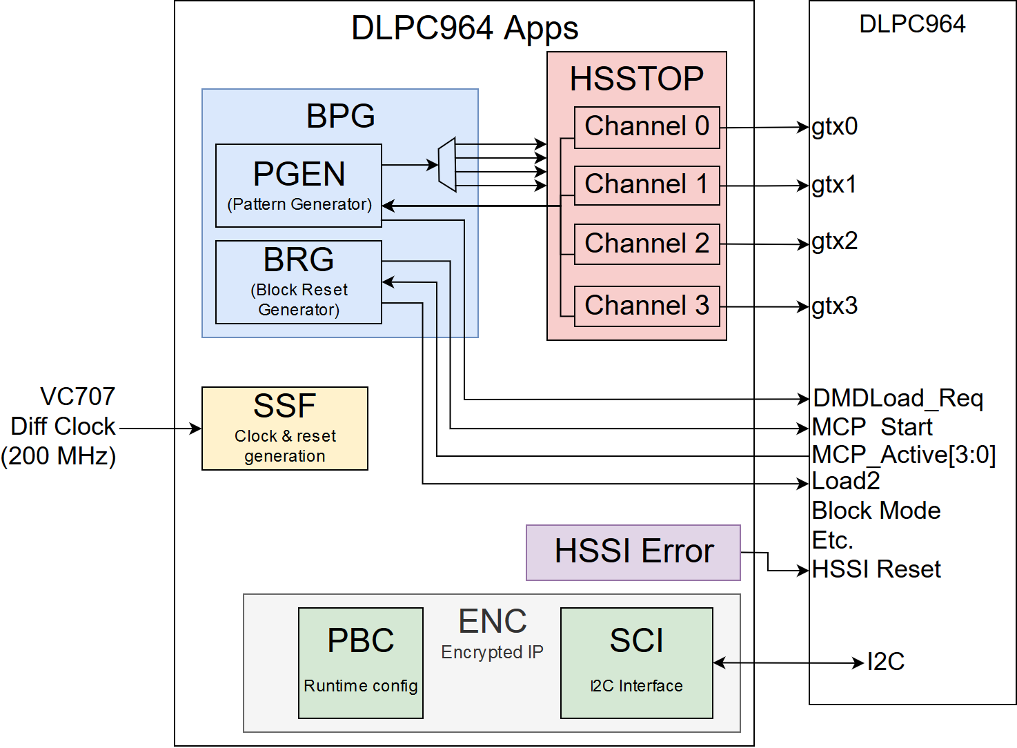
Figure 2-1 shows the Apps FPGA Hardware Block diagram with varies modules. Each module plays an important role in trasmitting bitplanes to the DLPC964 controller. The DLPC964 recieves high-speed bit plane data from the external front end source (AMD Xilinx Virtex-7 VC-707) and formats the data prior to loading into a DLPLCR99EVM or DLPLCR99UVEVM for display on a DLP991U or DLP991UUV DMD.
The Bitplane Pattern Generator (BPG) is the main module when interfacing with the DLPC964 Apps FPGA and helps monitor the bitplane data being loaded from PGEN into the DLPC964 controller. The Block Reset Generator (BRG) helps start the PGEN data that was sent to the DLPC964 when the controller is not busy which is determined by the mcp_active signal coming from the DLPC964 controller.
Once the data is ready to be loaded into PGEN, the bitplane data is transmitted through HSSTOP, which is a wrapper for all four GTX channels (gtx0 - gtx3). Each channel helps trasmit the bitplane data to the DLPC964 controller with speeds up to 10Gbps for each channel. These modules are going to be explained in further detail below.
 Figure 2-1 Apps FPGA Hardware Block Diagram