DLPU133 March 2024 DLPC964
- 1
- Abstract
- Trademarks
- 1Overview
-
2Apps FPGA
Modules
- 3.1 Apps FPGA Block Diagram
- 3.2 BPG Module
- 3.3 BRG Module
- 3.4 BRG_ST Module
- 3.5 PGEN Module
- 3.6 PGEN_MCTRL Module
- 3.7 PGEN_SCTRL Module
- 3.8 PGEN_PRM Module
- 3.9 PGEN_ADDR_ROM
- 3.10 HSSTOP Module
- 3.11 SSF Module
- 3.12 ENC Module
- 3.13 Xilinx IP
- 3.14 Reference Documents
- 3.15 DLPC964 Apps FPGA IO
- 3.16 Key Definitions
- 3Functional Configuration
-
4Appendix
- 5.1 Vivado Chipscope Captures
- 5.2 DLPC964 Apps Bitstream Loading
- 5.3
Interfacing To DLPC964 Controller with Aurora
64B/66B
- 5.3.1 Theory of Operation
- 5.3.2 Overview
- 5.3.3
Aurora 64B/66B TX Core and RTL Generation
- 5.3.3.1 Select Aurora 64B66B From IP Catalog
- 5.3.3.2 Configure Core Options
- 5.3.3.3 Lane Configurations
- 5.3.3.4 Shared Logic Options
- 5.3.3.5 Generate Example Design Files
- 5.3.3.6 RTL File List
- 5.3.3.7 Single Channel 3 Lanes Aurora Core RTL Wrapper
- 5.3.3.8 Four Channels 12 Lanes Top Level RTL Wrapper
- 5.3.3.9 Block Start with Block Control Word
- 5.3.3.10 Block Complete with DMDLOAD_REQ
- 5.3.3.11 DMDLOAD_REQ Setup Time Requirement
- 5.3.3.12 Single Channel Transfer Mode
- 5.3.3.13 DMD Block Array Data Mapping
- 5.3.3.14 Xilinx IBERT
- 5Abbreviations and Acronyms
- 6Related Documentation from Texas Instruments
2.2 BPG Module
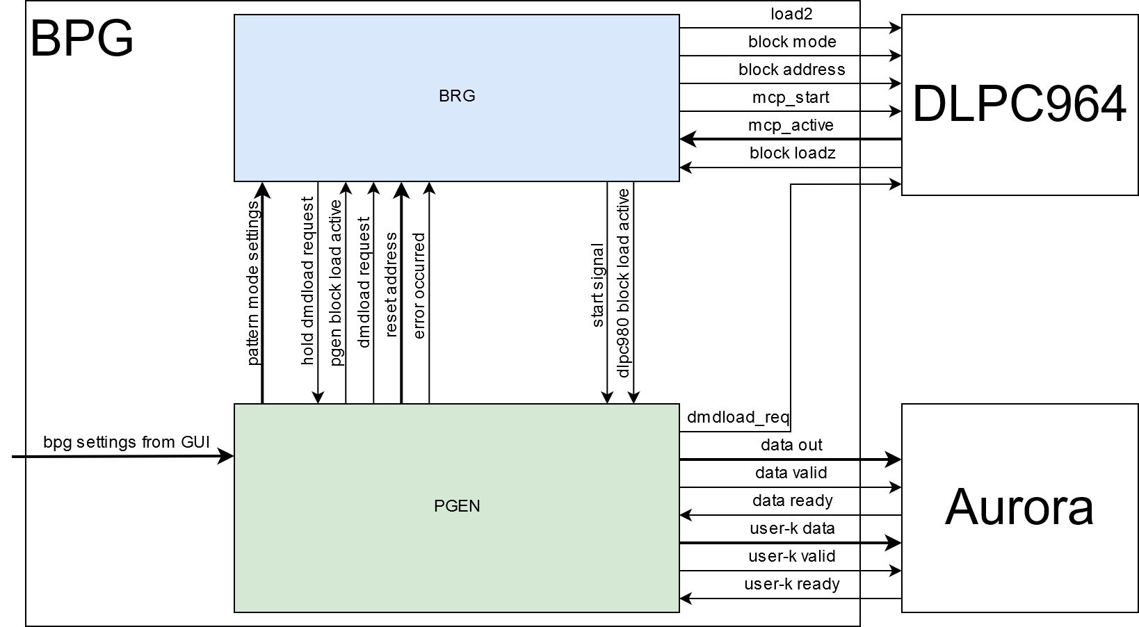
BPG (Bitplane Pattern Generator) is the main module of the DLPC964 Apps FPGA. This module can be used as an example on how to interface with the DLPC964 and Aurora transmit IP and consists of two main blocks:
- The BRG (Block Reset Generator)
- The PGEN (Pattern Generator)
The BPG acts as a wrapper for the two sub-blocks BRG and PGEN. The BRG sub-block is responsible for starting the PGEN and reporting when the DLPC964 is busy loading data.
The PGEN reports when sending data to the Aurora GTX IP, the next block address that is going to be reset from the DLPC964 with the mcp_start signal, errors that occur (timeout or DMD HSSI), and settings chosen from the user.
 Figure 2-2 BPG Module Hardware Block Diagram