DLPU133 March 2024 DLPC964
- 1
- Abstract
- Trademarks
- 1Overview
-
2Apps FPGA
Modules
- 3.1 Apps FPGA Block Diagram
- 3.2 BPG Module
- 3.3 BRG Module
- 3.4 BRG_ST Module
- 3.5 PGEN Module
- 3.6 PGEN_MCTRL Module
- 3.7 PGEN_SCTRL Module
- 3.8 PGEN_PRM Module
- 3.9 PGEN_ADDR_ROM
- 3.10 HSSTOP Module
- 3.11 SSF Module
- 3.12 ENC Module
- 3.13 Xilinx IP
- 3.14 Reference Documents
- 3.15 DLPC964 Apps FPGA IO
- 3.16 Key Definitions
- 3Functional Configuration
-
4Appendix
- 5.1 Vivado Chipscope Captures
- 5.2 DLPC964 Apps Bitstream Loading
- 5.3
Interfacing To DLPC964 Controller with Aurora
64B/66B
- 5.3.1 Theory of Operation
- 5.3.2 Overview
- 5.3.3
Aurora 64B/66B TX Core and RTL Generation
- 5.3.3.1 Select Aurora 64B66B From IP Catalog
- 5.3.3.2 Configure Core Options
- 5.3.3.3 Lane Configurations
- 5.3.3.4 Shared Logic Options
- 5.3.3.5 Generate Example Design Files
- 5.3.3.6 RTL File List
- 5.3.3.7 Single Channel 3 Lanes Aurora Core RTL Wrapper
- 5.3.3.8 Four Channels 12 Lanes Top Level RTL Wrapper
- 5.3.3.9 Block Start with Block Control Word
- 5.3.3.10 Block Complete with DMDLOAD_REQ
- 5.3.3.11 DMDLOAD_REQ Setup Time Requirement
- 5.3.3.12 Single Channel Transfer Mode
- 5.3.3.13 DMD Block Array Data Mapping
- 5.3.3.14 Xilinx IBERT
- 5Abbreviations and Acronyms
- 6Related Documentation from Texas Instruments
2.10 HSSTOP Module
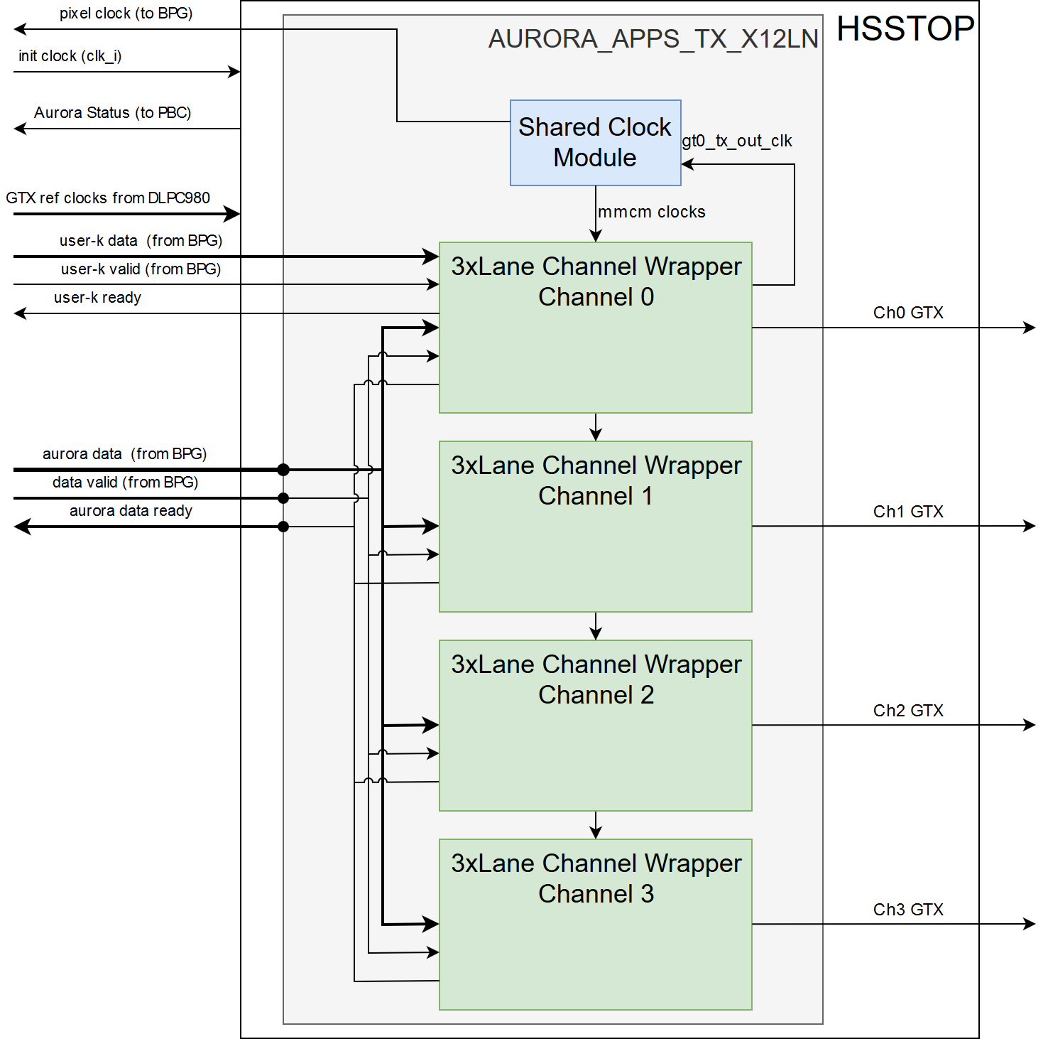
This module contains the Xilinx Aurora IP for transmitting bitplane data to the DLPC964 controller board. This protocal is called the Aurora 64b/66b and for more information, go to Section 4.3.
As shown in Figue 2-8, the HSSTOP module has an AURPRA_APPS_TX_X12LN wrapper for all four of the GTX channels. Each Aurora GTX channel is comprised of three lanes with each lane transmitting 10Gbps. To help keep the GTX lanes synchronized, all four of the channels share the same Aurora clock module.
 Figure 2-8 HSSTOP Module Hardware Block
Diagram
Figure 2-8 HSSTOP Module Hardware Block
DiagramThe Aurora IP allows the differential signals to have a pre-emphasis and post-emphasis to help with signal integrity. In the DLPC964 Apps FPGA design, the following settings were used.
| Signal Name | Value |
|---|---|
| gt_txpostcursor_in | 0.00dB (00000) |
| gt_txdiffctrl_in | 807mV (1000) |
| gt_txmaincursor_in | 0.00dB (00000) |
| gt_txprecursor_in | 0.00dB (00000) |