DLPU133 March 2024 DLPC964
- 1
- Abstract
- Trademarks
- 1Overview
-
2Apps FPGA
Modules
- 3.1 Apps FPGA Block Diagram
- 3.2 BPG Module
- 3.3 BRG Module
- 3.4 BRG_ST Module
- 3.5 PGEN Module
- 3.6 PGEN_MCTRL Module
- 3.7 PGEN_SCTRL Module
- 3.8 PGEN_PRM Module
- 3.9 PGEN_ADDR_ROM
- 3.10 HSSTOP Module
- 3.11 SSF Module
- 3.12 ENC Module
- 3.13 Xilinx IP
- 3.14 Reference Documents
- 3.15 DLPC964 Apps FPGA IO
- 3.16 Key Definitions
- 3Functional Configuration
-
4Appendix
- 5.1 Vivado Chipscope Captures
- 5.2 DLPC964 Apps Bitstream Loading
- 5.3
Interfacing To DLPC964 Controller with Aurora
64B/66B
- 5.3.1 Theory of Operation
- 5.3.2 Overview
- 5.3.3
Aurora 64B/66B TX Core and RTL Generation
- 5.3.3.1 Select Aurora 64B66B From IP Catalog
- 5.3.3.2 Configure Core Options
- 5.3.3.3 Lane Configurations
- 5.3.3.4 Shared Logic Options
- 5.3.3.5 Generate Example Design Files
- 5.3.3.6 RTL File List
- 5.3.3.7 Single Channel 3 Lanes Aurora Core RTL Wrapper
- 5.3.3.8 Four Channels 12 Lanes Top Level RTL Wrapper
- 5.3.3.9 Block Start with Block Control Word
- 5.3.3.10 Block Complete with DMDLOAD_REQ
- 5.3.3.11 DMDLOAD_REQ Setup Time Requirement
- 5.3.3.12 Single Channel Transfer Mode
- 5.3.3.13 DMD Block Array Data Mapping
- 5.3.3.14 Xilinx IBERT
- 5Abbreviations and Acronyms
- 6Related Documentation from Texas Instruments
3.2.5 Changing the BPG Patterns
Below are instructions to help users change the default patterns in the ROM for TPG selections.
- Go into the directory C:\Texas Instruments\DLPC964-Apps\docs\patterns and verify that the user has Python 2.6 (or greater) installed.
- Open the binary_to_coe.py
file and read through the top comments. The patterns used in the DLPC964
Apps were generated using this script. Look at the
bit_fnameslist located near the top of the script.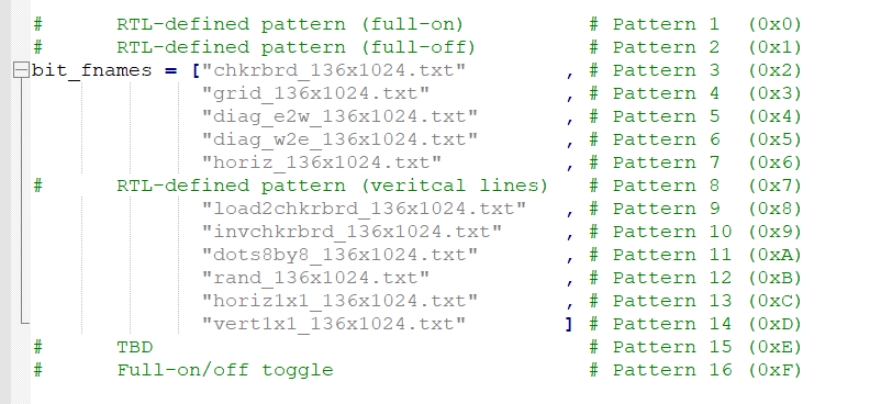
- The user can create a new .txt
file and replace one of the names within the
bit_fnameslist.Note: Any patterns designated RTL defined pattern cannot be changed to a different pattern since the patterns are not read from the ROM.- Instructions for creating
a .txt file for the python script:
- The text file MUST have 1024 columns and 136 lines.
- Each character in the text file must either be a '1' or a '0'.
- Make sure the text file is in the same directory as the python script.
- Instructions for creating
a .txt file for the python script:
- Once the
bit_fnameshas been updated with the new text file name, run the python script. This creates a file calledbpg_patterns.coe - Open the
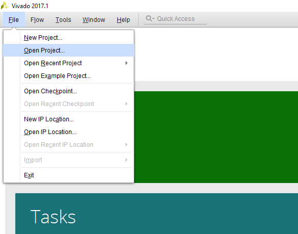
Vivado project (either by unzipping the archived project in the build\project
directory, or by running the run.tcl script).Note: Unzipping the project is faster but if desired, then the run.tcl script has instructions on how to run.
- Once the project is open, in the
Project Manager window, find the tab labeled IP sources and click.
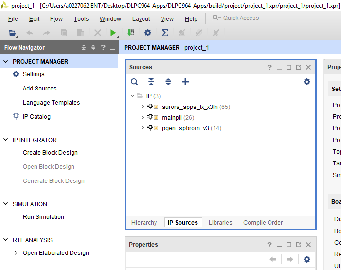
- Right-click on
pgen_spbrom_v3and select re-customize IP.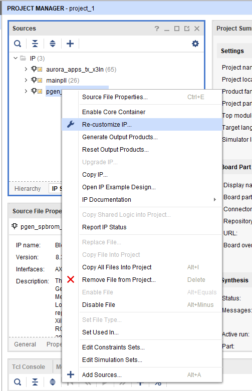
- Once the IP configuration tool is
open, go to the options tab and the user sees a Memory Initialization
section.
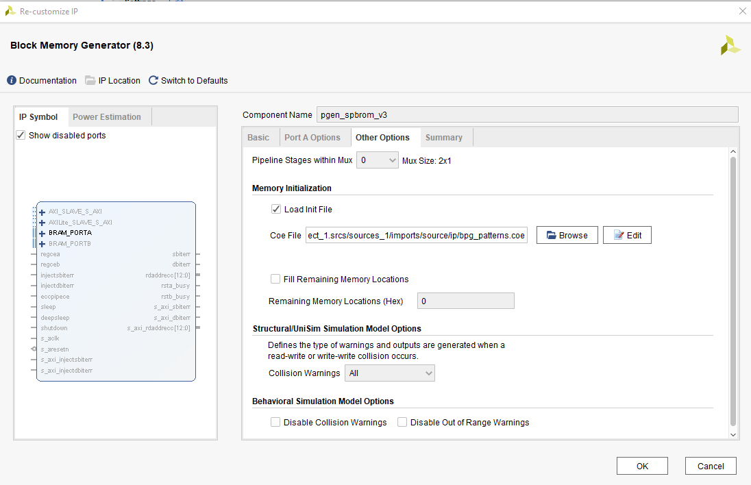
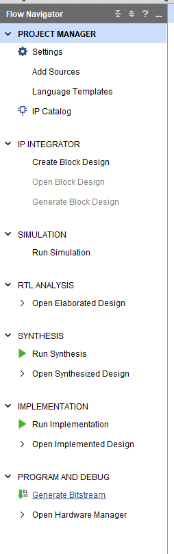
- Click Browse and navigate to the location of the bpg_patterns.coe file created by the python script in step 4. Assuming there are no errors, click OK. In the next window, click Generate.
- The user now has reprogrammed the ROM in the DLPC964 Apps FPGA. Now, re-build the project.
- Once
Xilinx finishes generating output products, click Generate Bitstream
located on the left in the Flow Navigator. Click OK to any prompts and
once Vivado finishes, the bitstream can be found inside the
project_1\project_1.runs\impl_1\ directory.