DLPU133 March 2024 DLPC964
- 1
- Abstract
- Trademarks
- 1Overview
-
2Apps FPGA
Modules
- 3.1 Apps FPGA Block Diagram
- 3.2 BPG Module
- 3.3 BRG Module
- 3.4 BRG_ST Module
- 3.5 PGEN Module
- 3.6 PGEN_MCTRL Module
- 3.7 PGEN_SCTRL Module
- 3.8 PGEN_PRM Module
- 3.9 PGEN_ADDR_ROM
- 3.10 HSSTOP Module
- 3.11 SSF Module
- 3.12 ENC Module
- 3.13 Xilinx IP
- 3.14 Reference Documents
- 3.15 DLPC964 Apps FPGA IO
- 3.16 Key Definitions
- 3Functional Configuration
-
4Appendix
- 5.1 Vivado Chipscope Captures
- 5.2 DLPC964 Apps Bitstream Loading
- 5.3
Interfacing To DLPC964 Controller with Aurora
64B/66B
- 5.3.1 Theory of Operation
- 5.3.2 Overview
- 5.3.3
Aurora 64B/66B TX Core and RTL Generation
- 5.3.3.1 Select Aurora 64B66B From IP Catalog
- 5.3.3.2 Configure Core Options
- 5.3.3.3 Lane Configurations
- 5.3.3.4 Shared Logic Options
- 5.3.3.5 Generate Example Design Files
- 5.3.3.6 RTL File List
- 5.3.3.7 Single Channel 3 Lanes Aurora Core RTL Wrapper
- 5.3.3.8 Four Channels 12 Lanes Top Level RTL Wrapper
- 5.3.3.9 Block Start with Block Control Word
- 5.3.3.10 Block Complete with DMDLOAD_REQ
- 5.3.3.11 DMDLOAD_REQ Setup Time Requirement
- 5.3.3.12 Single Channel Transfer Mode
- 5.3.3.13 DMD Block Array Data Mapping
- 5.3.3.14 Xilinx IBERT
- 5Abbreviations and Acronyms
- 6Related Documentation from Texas Instruments
4.3.3.11 DMDLOAD_REQ Setup Time Requirement
Apps FPGA user logics can assert the DMDLOAD_REQ signal as soon as completing an Aurora block transfer as long as the signal is at least 300ns after sending the first data packet of that block. This setup time requirement is due to the 300ns transmit latency of the Aurora TX/RX channel paths, thus verifies the DLPC964 receives the DMDLOAD_REQ flag after the arrival of Aurora block data.
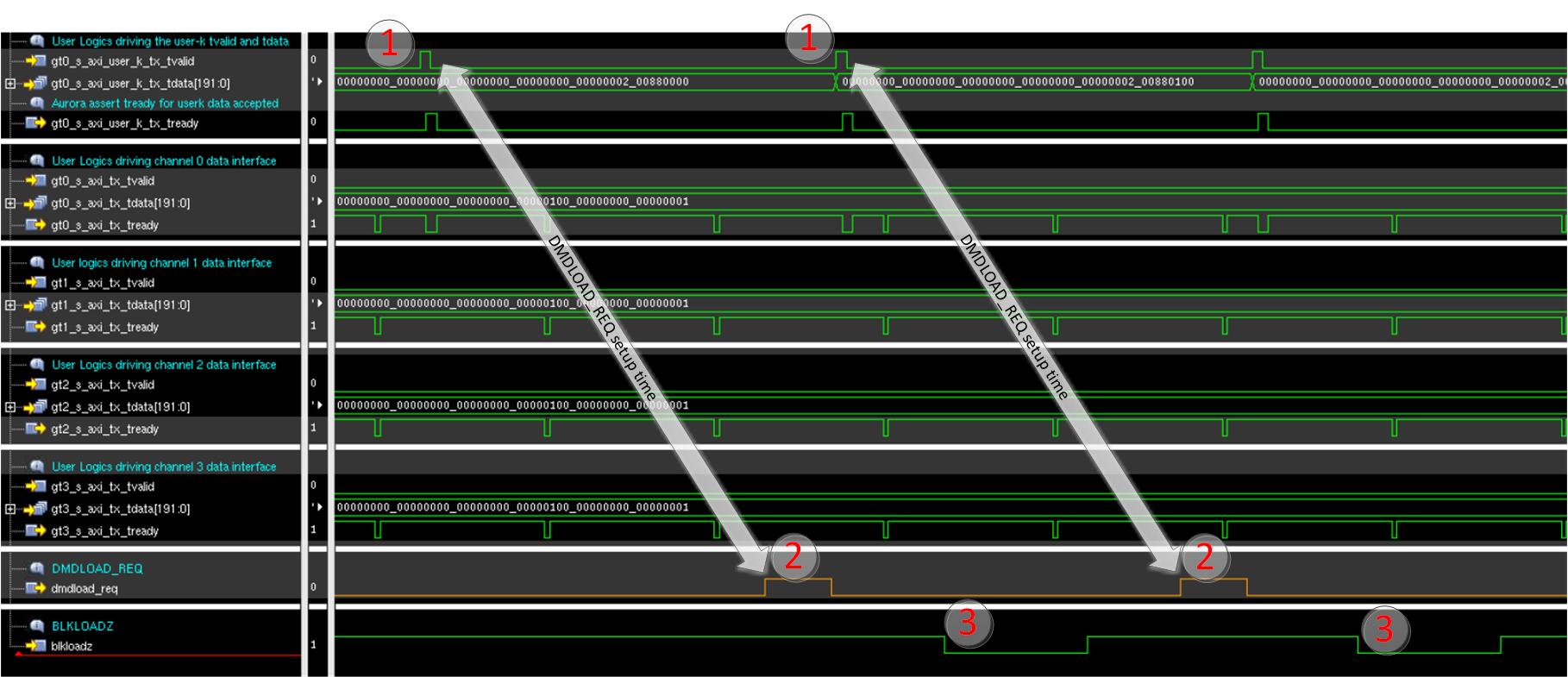
In most cases, this 300ns setup requirement is met naturally as a data block is large enough to verify over 300ns from the first valid data packet being sent to the last ones of a block when the Apps can assert the DMDLOAD_REQ signal. Cases of this 300ns setup window become critical is when Apps FPGA tries to send a small partial DMD block such as in Figure 4-21 showing an example of the Apps FPGA sending a total of 3 rows (Table 4-2 , ROW_LENGTH = 3) of a DMD partial block to DLPC964:
 Figure 4-21 DMDLOAD_REQ Setup Time for Three DMD Rows Load Operation
- Apps FPGA transmits a Block Control word to indicate the start of an Aurora block transfer.
- After sending three rows of data
through the four Aurora data interface channels, the Apps FPGA waits for the
300ns setup time to expire before issues a DMDLOAD_REQ. Note: The 300ns is measured from the start of the first TVALID on the data interface.
- Apps FPGA asserts DMDLOAD_REQ once the setup time is meet.
- BLKLOADZ asserted by DLPC964 indicating DMD data load operation in progress.
For operations that do not require the data packet, such as block clear (Table 3, LOAD_TYPE = 001) and block set (Table 3, LOAD_TYPE = 010). This DMDLOAD_REQ of 300ns setup time is still required and measured from the Block Control word packet. Figure 4-22 is an example of a block set operation.
 Figure 4-22 DMDLOAD_REQ Setup Time For Block Set Operation
- Apps FPGA transmits a Block Control word packet to start a block set operation. Notice this operation does not require any block data as the four data interfaces stay idle (gtX_s_axi_tx_tvalid = ‘0’).
- Apps FPGA asserts DMDLOAD_REQ after the 300ns setup time. 300ns is measured from Block Control word as block set operation does not require Aurora data transfer.
- DLPC964 asserts BLKLOADZ indicating block set operation in progress.