DLPU133A March 2024 – February 2025 DLPC964
- 1
- Abstract
- Trademarks
- 1Overview
-
2Apps FPGA
Modules
- 3.1 Apps FPGA Block Diagram
- 3.2 BPG Module
- 3.3 BRG Module
- 3.4 BRG_ST Module
- 3.5 PGEN Module
- 3.6 PGEN_MCTRL Module
- 3.7 PGEN_SCTRL Module
- 3.8 PGEN_PRM Module
- 3.9 PGEN_ADDR_ROM
- 3.10 HSSTOP Module
- 3.11 SSF Module
- 3.12 ENC Module
- 3.13 Xilinx IP
- 3.14 Reference Documents
- 3.15 DLPC964 Apps FPGA IO
- 3.16 Key Definitions
- 3Functional Configuration
-
4Appendix
- 5.1 Vivado Chipscope Captures
- 5.2 DLPC964 Apps Bitstream Loading
- 5.3
Interfacing To DLPC964 Controller with Aurora
64B/66B
- 5.3.1 Theory of Operation
- 5.3.2 Overview
- 5.3.3
Aurora 64B/66B TX Core and RTL Generation
- 5.3.3.1 Select Aurora 64B66B From IP Catalog
- 5.3.3.2 Configure Core Options
- 5.3.3.3 Lane Configurations
- 5.3.3.4 Shared Logic Options
- 5.3.3.5 Generate Example Design Files
- 5.3.3.6 RTL File List
- 5.3.3.7 Single Channel 3 Lanes Aurora Core RTL Wrapper
- 5.3.3.8 Four Channels 12 Lanes Top Level RTL Wrapper
- 5.3.3.9 Block Start with Block Control Word
- 5.3.3.10 Block Complete with DMDLOAD_REQ
- 5.3.3.11 DMDLOAD_REQ Setup Time Requirement
- 5.3.3.12 Single Channel Transfer Mode
- 5.3.3.13 DMD Block Array Data Mapping
- 5.3.3.14 Xilinx IBERT
- 5Abbreviations and Acronyms
- 6Related Documentation from Texas Instruments
- 7Revision History
2.7 PGEN_SCTRL Module
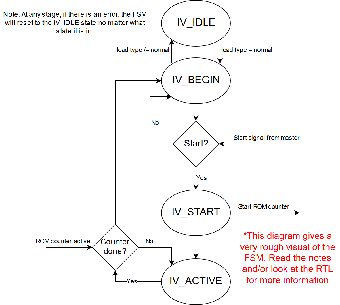
There are four copies of the secondary control module that are controlled by the primary control module. Each secondary is responsible for sending out the proper length data valid signal and to increment the ROM address. The data valid signal goes to the Aurora interface to mark the data being sent as valid. The Aurora interface can de-assert the ready signal at various times, so the secondary module must take this into account by holding the values and valid signal until the ready signal is re-asserted. The maximum ROM address is sent to the secondary module by the primary control module. The secondary module counts up to this value allowing the ROMs to send out lines up to the user-specified amount. Figure 2-7 depicts the main Secondary FSM where each state machine is defined as followed:
- IV_IDLE - When the secondary modules are not needed (for example, when load types clear or set are selected), the secondary module is held in this idle state. If data is needed (load type = Normal), then the FSM goes to the next state.
- IV_BEGIN - Wait until the primary module sends a start signal. Once received, the secondary goes to the next state. Otherwise, the FSM holds in this state until the FSM receives the start signal OR the load type is changed.
- IV_START - The FSM starts the process to send out the valid signal and the ROM addresses. The valid signal is delayed a few clock cycles to align the ROM output with the valid signal.
- IV_ACTIVE - Once the secondary module is started, the process that outputs ROM addresses continues to run until the module has reached the ROM address sen by the primary module. Once the value is reached, the FSM is signaled to go to beginning state.
 Figure 2-7 PGEN_SCTRL FSM