SBAA265A October 2018 – September 2024 ADS8912B , OPA320
| Input | ADC Differential Input (Vdif) | ADC Common-Mode Input (Vcm) | Digital Output ADS9110 |
|---|---|---|---|
| 0V | –5V | 2.5V | 20000H |
| 5V | +5V | 2.5V | 1FFFFH |
| V+ (op amp) | AVDD | DVDD | REFP |
|---|---|---|---|
| 5V | 5V | 3V | 5V |
Design Description
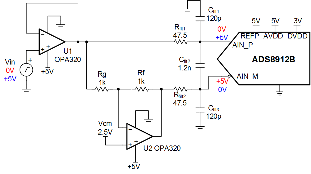
This circuit uses two OPA320 op amps to perform a single-ended to differential conversion for driving the ADS8912B fully-differential ADC. Another approach to solve this problem uses a fully-differential amplifier (FDA). See Single-Ended to Differential Conversion Using an Op Amp and FDA for Unipolar Signals for the FDA example. Since there are many thousands of different types of op amps available, finding an op amp the meets your specific requirements may be easer than finding an fully-differential amplifier. Most FDAs, for example, do not have as good swing to the rail, offset, bias current, and drift as many precision op amps have. On the other hand, the op-amp approach has an asymmetrical group delay in the inverting and non-inverting paths. Furthermore, FDA amplifiers often have better distortion and ADC drive characteristics. In general, the FDA approach will achieve best SNR and THD, and the op-amp approach will achieve best DC characteristics. Nevertheless, the specific op amp or FDA will impact the comparison of the two typologies.
Specifications
| Specification | Goal | Calculated | Simulated |
|---|---|---|---|
| Transient ADC Input Settling (1MSPS) | < 0.5LSB = 19.1µV | NA | 5µV |
| Input Output Range | NA | NA | 0.1 < VIN < 4.9V –4.8V < VOUT < 4.8V |
| Noise | NA | 30.5µVRMS | 28.4µVRMS |
Design Notes
- Use 0.1% resistors for R1 and Rg to minimize gain error and drift on U2.
- Select COG (NPO) capacitors for Cfilt1, Cfilt2, and Cfilt3 to minimize distortion.
- The Precision labs series: Analog-to-digital converters (ADCs)training video series covers methods for selecting the charge bucket circuit Rfilt and Cfilt. These component values are dependent on the amplifier bandwidth, data converter sampling rate, and data converter design. The values shown here will give good settling and AC performance for the amplifier and data converter in this example. If you modify this design you will need to select a different RC filter. See the Introduction to SAR ADC Front-End Component Selection training video for an explanation of how to select the RC filter for best settling and AC performance.
Component Selection
- Select an op amp to meet the system
requirements. Key specifications to consider follow:
- Swing to rail - For 5-V supply rails it is common to use a rail-to-rail zero crossover distortion device (for example, OPA320, OPA325, and OPA365).
- Offset voltage and Drift - One of the advantages of this circuit over the FDA approach is that some op-amps can have very good DC performance.
- Bandwidth and quiescent current - Another advantage of this circuit over the FDA approach is that a wide range of op-amp bandwidth and related quiescent currents are available. For lower sampling rate a low bandwidth low current op amp may be a good choice.
- Choose Rg and Rf to minimize noise. The gain of this circuit is always 1, so Rg = Rf. The main consideration here is to minimize noise while keeping the load resistance reasonable. Set the resistor noise to be roughly ⅓ of the amplifier noise. In this example Rf = Rg = 1kΩ gives a noise of 2.8nV/√ Hz which is approximately ⅓ of the 7nV/√ Hz op-amp noise. Also, the maximum load current is 2.5mA (5V ÷ 2kΩ = 2.5mA) which is low compared to the op-amp short-circuit limit (65mA).
- Find Rfilt and Cfilt to allow for settling at 1kSPS. See Refine the Rfilt and Cfilt Values for the algorithm to select Rfilt and Cfilt. The final value of 200kΩ and 510pF proved to settle to well below ½ of a least significant bit (LSB).
DC Transfer Characteristics
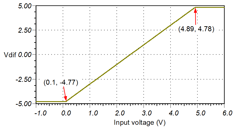
The following graph shows the DC transfer characteristics for this circuit (0-V to 5-V single-ended input, –5-V to +5-V fully-differential output). Note that the linear range is limited to about 0.1V from both supply rails (Vin linear range approximately 0.1V to 4.9V). The limitation is from the amplifier output swing limit. For improved linear swing the negative and positive supply on the amplifiers would need to be adjusted. See Low-Power Sensor Measurements: 3.3-V, 1-ksps, 12-bit, Single-Ended, Dual-Supply Circuit for an example on how to do this.
AC Transfer Characteristics
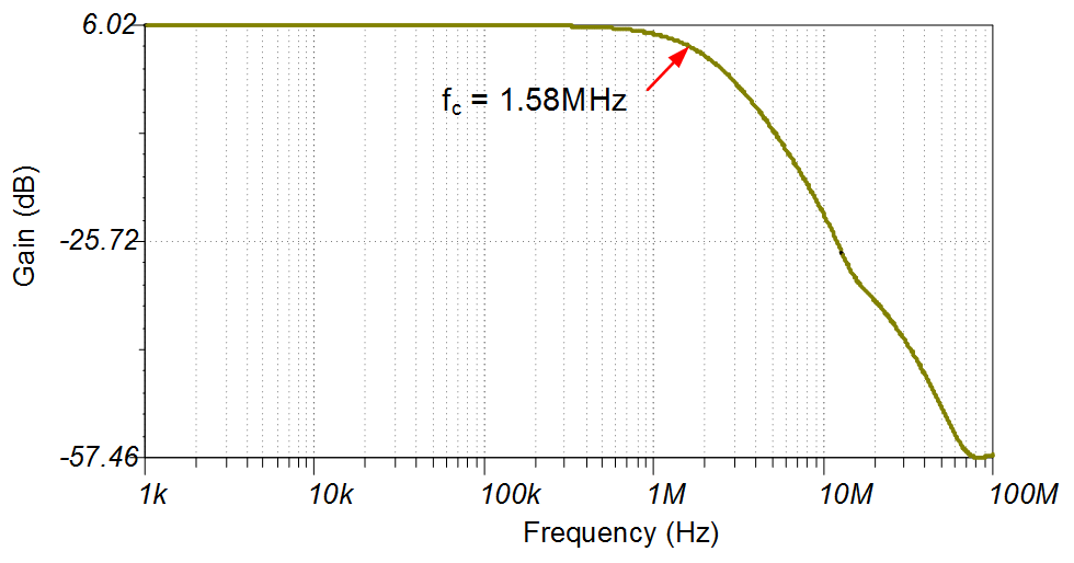
In this case the bandwidth limitation is primary set by the Rfilt, Cfilt values. The amplifier closed loop bandwidth can also impact the overall bandwidth. Note the bandwidth of U2 is half the bandwidth of U1 as its noise gain is two (BWU2 = GBW/Gn = 20MHz/2 = 10MHz).

Group Delay (Frequency Domain)
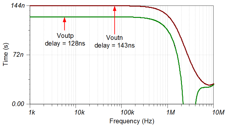
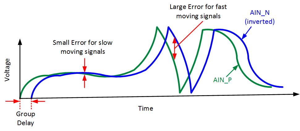
Group delay is the time delay between the applied input signal and the output signal. All amplifiers and filters will have a group delay. Group delay is highlighted for this circuit because the inverting and non-inverting path both have different group delays. This can create distortion for higher frequency signals. See the group delay in time domain plot for additional detail.
Group Delay (Time Domain)
The following graph shows qualitatively how group delay can effect time domain signals. The errors in this plot are exaggerated to emphasize the effect of group delay. The green signal represents the output on AIN_P and the blue signal represents the inverted output on AIN_N. Ideally, the two signals should track, but the group delay shifts the blue signal to the right. Notice that when signals are moving slowly the error is relatively small and when they are moving rapidly the error is larger. Thus, low frequency signals will have good distortion, and higher frequency signals will have degraded distortion. SPICE does not simulate THD, so for quantitative values measurement is required. However, if the input signal period more than 1,000 times larger than the group delay between the channels than this effect can generally be neglected.
Noise Simulation
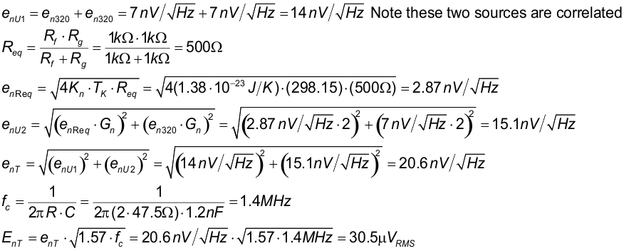
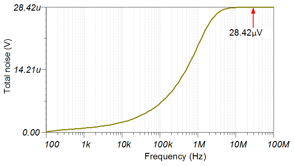
The following noise calculation considers the amplifier and resistor noise. Note that the noise from U1 is inverted by U2 and added at the differential output. Since this noise is directly correlated, it adds directly as opposed to root sum square addition usually used for noise sources. Also note that the output filter is approximated as first order but it is a more complex filter. The calculated noise compares well to the simulated noise (calculated = 30.5µVRMS, simulated = 28.4µVRMS).
The calculated noise compares well to the simulated noise (calculated = 30.5µVRMS, simulated = 28.4µVRMS). See Calculating the Total Noise for ADC Systems for detailed theory on this subject.
Transient ADC Input Settling Simulation
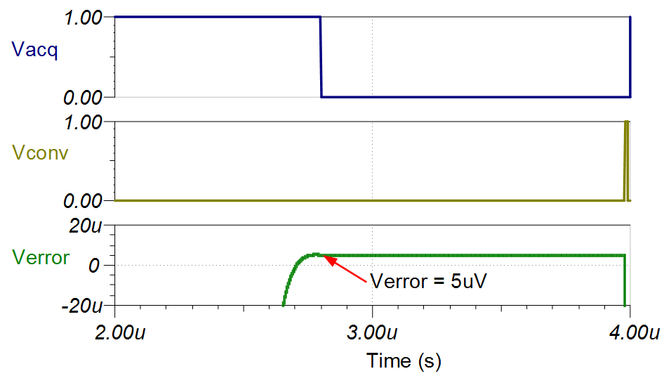
The following simulation shows settling to a full scale DC input signal at 500kSPS. This type of simulation shows that the sample and hold kickback circuit is properly selected. See Introduction to SAR ADC Front-End Component Selection for detailed theory on this subject.
Design Featured Devices
| Device | Key Features | Link | Other Possible Devices |
|---|---|---|---|
| ADS8912 | 18-bit resolution, 500-kSPS sample rate, integrated reference buffer, fully-differential input, Vref input range 2.5V to 5V. | 18-Bit, 500kSPS, 1-Ch SAR ADC with Internal VREF Buffer, Internal LDO and Enhanced SPI Interface | Precision ADCs |
| OPA320 | 20-MHz bandwidth, Rail-to-Rail with zero crossover distortion, VosMax = 150μV, VosDriftMax = 5μV/C, en = 7 nV/√ Hz | Precision, zero-crossover, 20MHz, 0.9pA Ib, RRIO, CMOS operational amplifier | Precision op amps (Vos < 1mV) |
Link to Key Files
Texas Instruments, source files for SBAA265, support software