SBAA267B February 2018 – September 2024 ADS8912B , OPA197 , REF5045 , THS4551
| Input Voltage (OPA197 Buffers) | THS4551 Output, ADC Input | ADS8912B Digital Output |
|---|---|---|
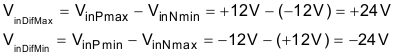
| VinP = –12V, VinN = +12V, VinMin (Dif) = –24V | VoutDif = –4.00V, VoutP = 0.25V, VoutN = 4.25V | 238E3H -11650910 |
| VinP = +12V, VinN = –12V, VinMax (Dif) = +24V | VoutDif = +4.0V, VoutP = 4.25V, VoutN = 0.25V | 1C71CH +11650810 |
| HVDD | HVSS | Vcc | Vee | Vref | Vcm |
|---|---|---|---|---|---|
| +15V | –15V | +5.0V | 0V | +4.5V | 2.5V |
Design Description
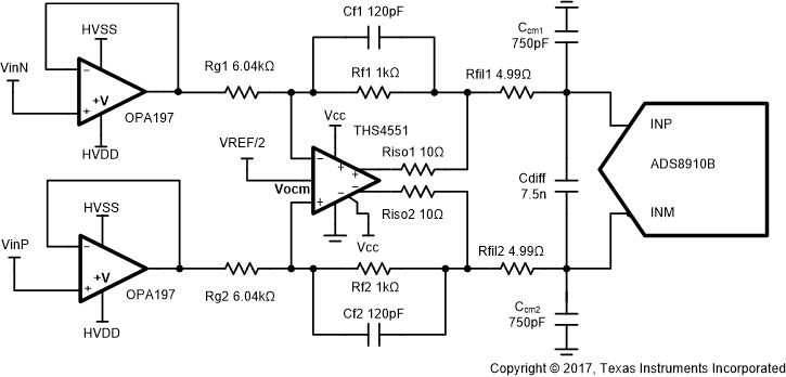
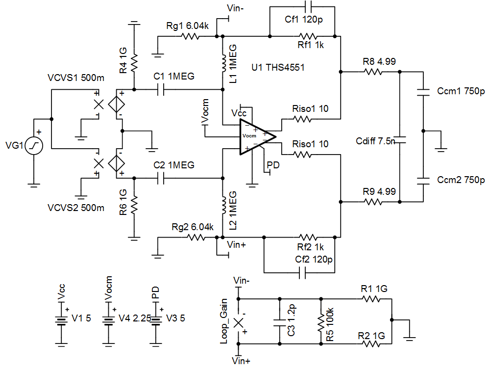
This analog front end (AFE) and SAR ADC data acquisition solution can measure true differential voltage signals in the range of ±24V (or absolute input range VinP = ±12V, VinN = ±12V) offering high-input impedance supporting data rates up to 500ksps with 18-bit resolution. A precision, 36-V rail-to-rail amplifier with low-input bias current is used to buffer the inputs of a fully-differential amplifier (FDA). The FDA attenuates and shifts the signal to the differential voltage and common-mode voltage range of the SAR ADC. The values in the component selection section can be adjusted to allow for different input voltage levels.
This circuit implementation is used in accurate measurement of true differential voltage in parametric measurement units (PMUs), precision multifunction input and output DAQs, and analog input modules used in Programmable Automation Control (PAC), Discrete Control System (DCS), and Programmable Logic Control (PLC) applications.
| Specification | Goal | Calculated | Simulated |
|---|---|---|---|
| Transient ADC Input Settling (500ksps) | << 1 LSB; << 34µV | N/A | 0.5µV |
| Noise (at ADC Input) | 10µVRMS | 9.28µVRMS | 9.76µVRMS |
| Bandwidth | 1.25MHz | 1.25MHz | 1.1MHz |
Design Notes
- Verify the linear range of the op amp (buffer) based on the common mode, output swing specification for linear operation. This is covered in the component selection section. Select an amplifier with low input bias current.
- Find ADC full-scale range and common-mode range specifications. This is covered in the component selection.
- Determine the required attenuation for the FDA based on the input signal amplitude, the ADC full-scale range and the output swing specifications of the FDA. This is covered in the component selection section.
- Select COG capacitors to minimize distortion.
- Use 0.1% 20ppm/°C film resistors or better for good accuracy, low gain drift, and to minimize distortion.
- Understanding and Calibrating the Offset and Gain for ADC Systems covers methods for error analysis. Review the link for methods to minimize gain, offset, drift, and noise errors
- Introduction to SAR ADC Front-End Component Selection covers methods for selecting the charge bucket circuit Rfilt and Cfilt. These component values are dependent on the amplifier bandwidth, data converter sampling rate, and data converter design. The values shown here will give good settling and AC performance for the amplifier, gain settings, and data converter in this example. If the design is modified, a different RC filter must be selected. Refer to the Precision Labs videos for an explanation of how to select the RC filter for best settling and AC performance.
Component Selection and Settings for Buffer Amplifier and FDA
- Verify the buffer amplifier
input range for linear operation:
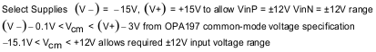
- Verify the buffer amplifier
output range for linear operation:

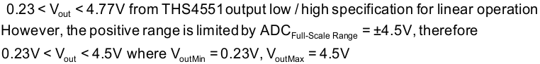
- Find ADC full-scale input
range. In this circuit, VREF = 4.5V:

- Find the required ADC
common-mode voltage:

- Find FDA absolute output
voltage range for linear operation:
- Find FDA differential output
voltage range for linear operation. The general output voltage equations for
this circuit follow:
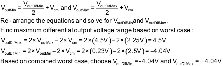
- Find the FDA differential input
voltage range:
- Find FDA required attenuation
ratio:
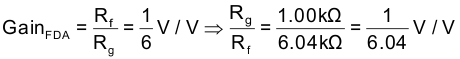
- Find standard resistor values
to set the attenuation:
- Find Cƒ for cutoff
frequency ƒc, RfINA = 1kΩ:

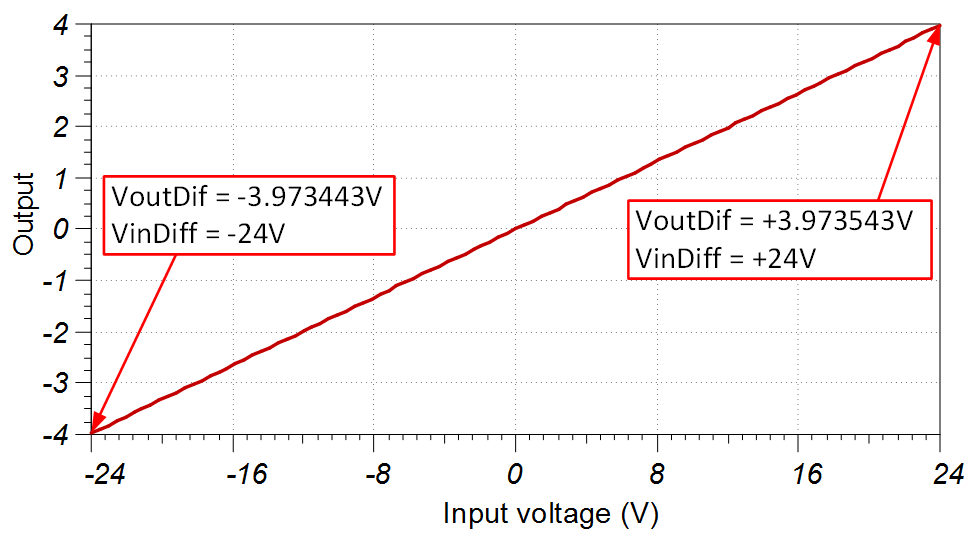
DC Transfer Characteristics
The following graph shows a linear output response for differential inputs from +24V to –24V.
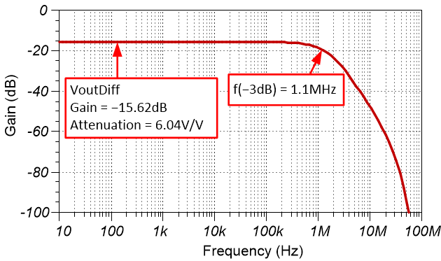
AC Transfer Characteristics
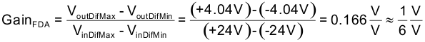
The simulated bandwidth is approximately 1.1MHz and the gain is –15.62dB which is a linear gain of approximately 0.166V/V (attenuation ratio 6.04V/V).
Noise Simulation
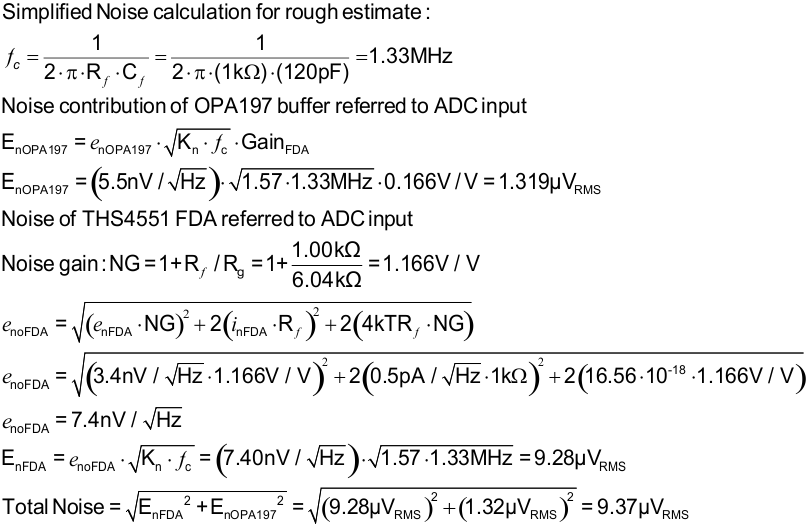
Note that calculated and simulated match well. Refer to Calculating the Total Noise for ADC Systems for detailed theory on this subject.

Stability Simulation
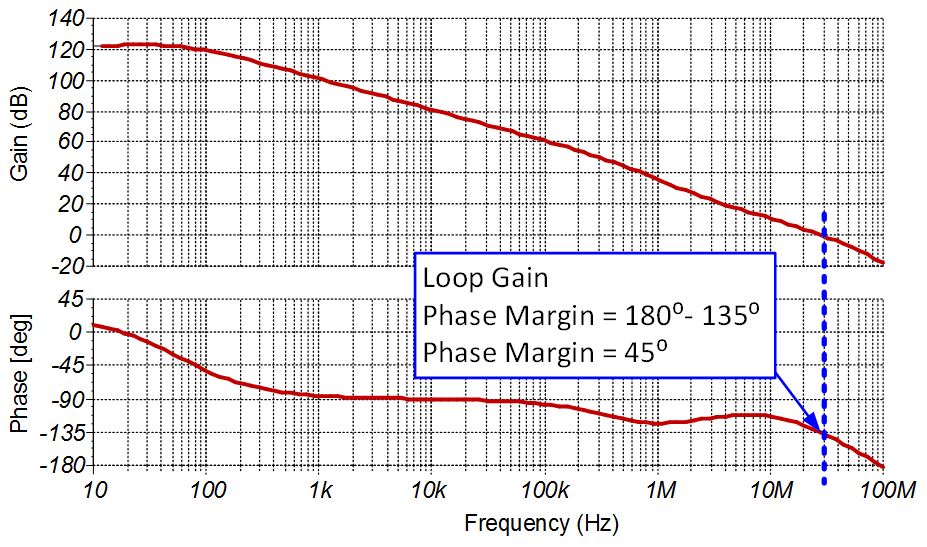
The following circuit is used in TINA to measure loop gain and verify phase margin using AC transfer analysis in TINA. Resistors RISO = 10Ω are used inside the feedback loop to increase phase margin. The circuit has 45 degrees of phase margin. Refer to TI Precision Labs - Op Amps: Stability 4 for detailed theory on this subject.
Transient ADC Input Settling Simulation
The following simulation shows settling to a 24-V DC differential input signal with the OPA197 buffers inputs set at +12V and –12V. This type of simulation shows that the sample and hold kickback circuit is properly selected. Refer to Refine the Rfilt and Cfilt Values for detailed theory on this subject.

Design Featured Devices
| Device | Key Features | Link | Similar Devices |
|---|---|---|---|
| ADS8912B(1) | 18-bit resolution, 500-ksps sample rate, integrated reference buffer, fully-differential input, Vref input range 2.5V to 5V. | 18-Bit, 1MSPS, 1-Ch SAR ADC with Internal VREF Buffer, Internal LDO and Enhanced SPI Interface | Analog-to-digital converters (ADCs) |
| THS4551 | FDA, 150-MHz bandwidth, Rail-to-Rail Output, VosDriftMax = 1.8µV/°C, en = 3.3nV/rtHz | Low Noise, Precision, 150MHz, Fully Differential Amplifier | Operational amplifiers (op amps) |
| OPA197 | 36V, 10-MHz bandwidth, Rail-to-Rail Input/Output, VosMax = ±250µV, VosDriftMax = ±2.5µV/°C, bias current = ±5pA | Single, 36V, precision, rail-to-rail input output, low offset voltage op amp | Operational amplifiers (op amps) |
| REF5045 | VREF = 4.5V, 3 ppm/°C drift, 0.05% initial accuracy, 4µVpp/V noise | 4.5V, 3-µVpp/V noise, 3-ppm/°C drift precision series voltage reference | Series voltage references |
Link to Key Files
Texas Instruments, SBAC183 source files, software support