SBAA286A October 2018 – September 2024 ADS8528 , ADS8548 , ADS8568 , INA828 , LMH6642 , LMH6643 , LMH6643Q-Q1 , LMH6644 , OPA2863 , OPA2863A , OPA827 , OPA863 , OPA863A
| Input | ADC Input | Digital Output ADS7042 |
|---|---|---|
| VinDiffMin = –10V | CH_x = –10V | 8000H |
| VinDiffMax = +10V | CH_x = +10V | 7FFFH |
| AVDD | DVDD | HVDD (VCC) | HVSS(VEE) |
|---|---|---|---|
| 5.0V | 3.3V | +15V | –15V |
Design Description
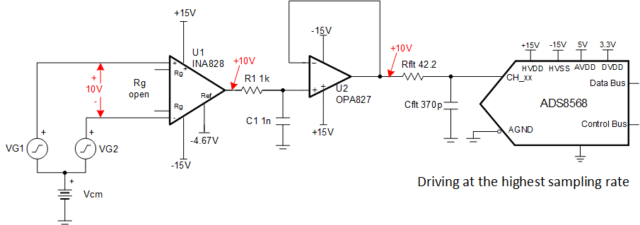
Instrumentation amplifiers are optimized for low noise, low offset, low drift, high CMRR and high accuracy but these instrument amplifiers may not be able to drive a precision ADC to settle the signal properly during the acquisition time of ADC. This design will show how a wide bandwidth buffer (OPA827) can be used with an instrumentation amplifier to achieve good settling at higher sampling rate. This INA828 instrumentation amplifier with the buffer drives the ADS8568 SAR ADC to implement data capture for a high voltage fully differential signal which may have a wide common-mode voltage range or a bipolar single-ended signal up to ±10V. A related cookbook circuit shows a simplified approach that does not include the wide bandwidth buffer (Driving High Voltage SAR ADC with an Instrumentation Amplifier), this simplified approach has limited sampling rate as compared to the buffered design in this document. This circuit implementation is applicable to industrial transportation and analog input modules that require Precision Signal-Processing and Data-Conversion.
Specifications
| Specification | Goal | Calculated | Simulated |
|---|---|---|---|
| Transient Settling Error | < 1/2LSB (< 152µV) | NA | –346nV |
| Noise (at ADC Input) | <20µVRMS | 47.2µVRMS | 46µVRMS |
Design Notes
- The bandwidth of instrumentation amplifiers is typically not enough to drive SAR data converters at higher data rate, so a wide bandwidth driver is needed because the SAR ADC with switched-capacitor input structure has an input capacitor that needs to be fully charged during each acquisition time. The OPA827 buffer is added to allow the ADC to run at full sampling rate (ADS8568 510kSPS for parallel interface).
- The ADS8568 can accept a ±10-V single-ended input signal. The INA828 is used to translate a ±10-V differential signal to a ±10-V single-ended signal. So the INA282 is in unity gain for this example, and no external gain set resistor Rg is needed. Refer to Circuit for Driving an ADC with an Instrumentation Amplifier in High Gain in cases where the input signal range is small and gain is required.
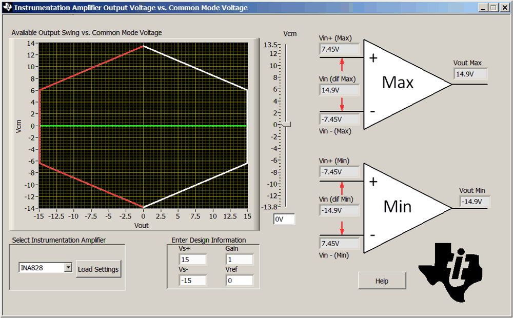
- Check the common mode range of the amplifier using the analog engineer's calculator.
- Select COG capacitors for C1 and Cfilt to minimize distortion.
- Precision labs video series covers the method for selecting driver amplifier and the charge bucket circuit Rfilt and Cfilt. For details, see the Selecting and Verifying the Driver Amplifier and Introduction of SAR ADC Front-End Component Selection videos.
- Set the cutoff of the filter between the op amp and instrumentation amplifier for anti aliasing and to minimize noise. See Aliasing and Anti-aliasing Filters for more details on aliasing and anti-aliasing filters.
Component Selection
- Find the gain based on differential input signal and ADC full-scale input range. The input signal in this design is ±10V high voltage signal, so the Gain of INA828 should be set to 1 and no gain resistor (Rg) is needed.
- Use the analog
engineer's calculator to determine if the INA828 is
violating the common mode range. The common mode calculator in the following
figure indicates that the output swing is ±14.9V for a 0-V common-mode input.
- Find the value for Cfilt, and Rfilt using TINA SPICE and the methods described in SAR ADC Front-End Component Selection. The value of Rfilt and Cfilt shown in this document will work for these circuits; however, if you use different amplifiers you will have to use TINA SPICE to find new values.
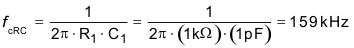
- Select the RC filter between the
INA828 and OPA827 based
on your system requirements (fcRC = 15.9kHz in this example). Set the
cutoff of this filter for anti aliasing and to minimize noise.
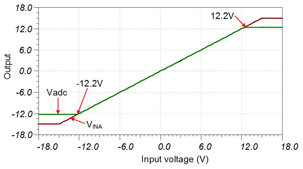
DC Transfer Characteristics
The following graph shows a linear output response for inputs from differential –12.2V to +12.2V. The input range of the ADC is ±10V, so the amplifiers are linear well beyond the required range. Refer to Determining a SAR ADC’s Linear Range when using Instrumentation Amplifiers for detailed theory on this subject. The full-scale range (FSR) of the ADC falls within the linear range of the Instrumentation Amplifier.
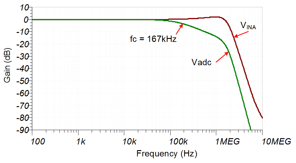
AC Transfer Characteristics
The bandwidth for this system is simulated to be 167kHz and the gain is 0dB. The filter between the OPA827 and INA828 limits the bandwidth to about 167kHz.
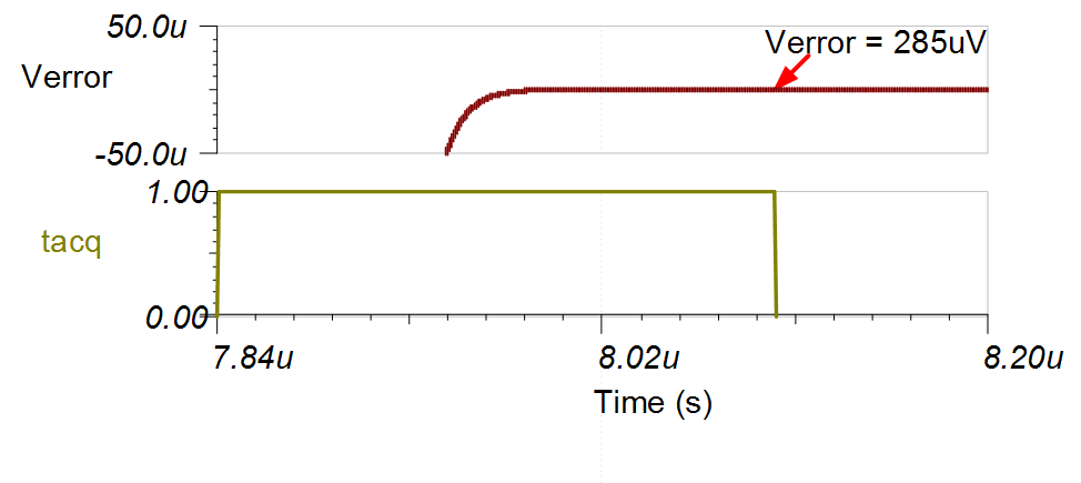
Transient ADC Input Settling Simulation (510kSPS)
The OPA827 buffer (22MHz GBW) is used because it is capable of responding to the rapid transients from the charge kickback fromADS8568. The op amp buffer allows the system to achieve the ADS8568 maximum sampling rate of 510kSPS. The following simulation shows settling to a full scale DC input signal with INA828 and OPA827 buffer, and ADS8568.. This type of simulation shows that the sample and hold kickback circuit is properly selected to meet desired ½ of a LSB (152µV). Refer to the Introduction to SAR ADC Front-End Component Selection training video series for detailed theory on this subject.
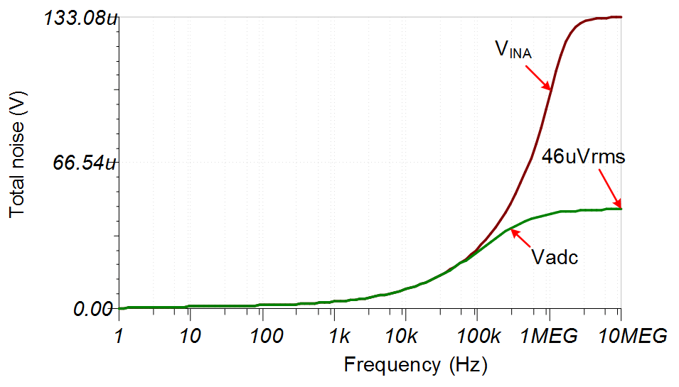
Noise Simulation
The section walks through a simplified noise calculation for a rough estimate. We include both the INA828 and OPA827 noise. Note that the RC filter between the instrumentation amplifier and op amp significantly reduces the total noise. The output filter pole is estimated as a second order filter because the OPA827 (22MHz) bandwidth limit and charge bucket filter cutoff frequency (10.2MHz) is close.
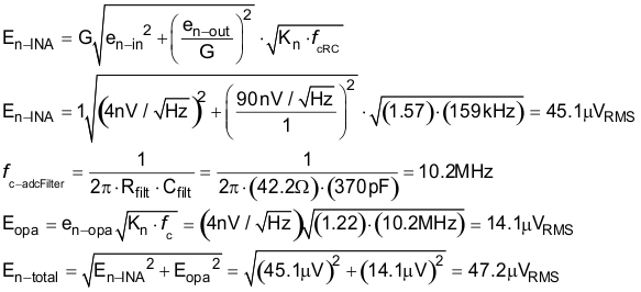
Note that calculated and simulated match well- (calculated = 47.2µV, Simulated = 46µV). See TI Precision Labs for detailed theory on amplifier noise calculations, and Calculating Total Noise for ADC Systems for data converter noise.
Design Featured Devices
| Device | Key Features | Link | Similar Devices |
|---|---|---|---|
| ADS8568 | 16-bit, 8 Channel Simultaneous-Sampling, Bipolar-Input SAR ADC | 16-bit, 8-channel, simultaneous-sampling, bipolar-input, SAR analog-to-digital converter (ADC) | Analog-to-digital converters (ADCs) |
| INA828 |
Bandwidth 1MHz (G=1), low noise 18nV/rtHz, low offset ±40μV, low offset drift ±0.4μV/°C, low gain drift 0.1ppm/°C (Typical values) |
50-μV Offset, 7-nV/√Hz Noise, Low-Power, Precision Instrumentation Amplifier | Instrumentation amplifiers |
| OPA827 | Gain bandwidth 22MHz, low noise 4nV/rtHz, low offset ±75μV, low offset drift ±0.1μV/°C (Typical values) | Low-noise, high-precision, JFET-input operational amplifier | Operational amplifiers (op amps) |
Links to Key Files
Texas Instruments, sources files for SBAA286, support software