SBAA312A September 2018 – June 2024 ADS7945 , ISO224 , REF5050
| ISO224 Input Voltage | ISO Output, ADC Input (VOUTP - VOUTN) | Digital Output ADS7945 |
|---|---|---|
| +12V | +4V | 1999H |
| –12V | –4V | E666H |
| Power Supplies and Reference Voltages | ||
|---|---|---|
| VDD1 | VDD2 and AVDD | REF5050 External Ref |
| 15V | 5V | 5V |
Design Description
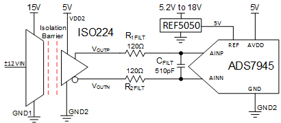
This circuit performs a ±12-V isolated voltage sensing measurement utilizing the ISO224 isolated amplifier and the ADS745 SAR ADC. The ISO224 can measure true differential signals of ±12V with a fixed gain of ⅓V/V and produces an isolated differential output voltage with an output common-mode voltage of VDD2 / 2. The ADS7945 is a fully differential input ADC with a full-scale input voltage of ±VREF and a common-mode input voltage of VREF / 2 ±200mV. Selecting a +5-V reference allows the ADS7945 to accept the full-scale and common-mode outputs from the ISO224. Capturing the ISO224 output with a fully differential input ADC doubles the system dynamic range compared to a single-ended conversion. Many high-voltage industrial applications such as Protection Relays, Channel-to-Channel Isolated ±10V Analog Input Cards, and Inverter & Motor Control. The equations and explanation of component selection in this design can be customized based on system specifications and needs.
Specifications
| Specification | Calculated | Simulated |
|---|---|---|
| Transient ADC input settling at 100ksps | 305µV | 11µV |
| Conditioned signal range | ±4V | ±4V |
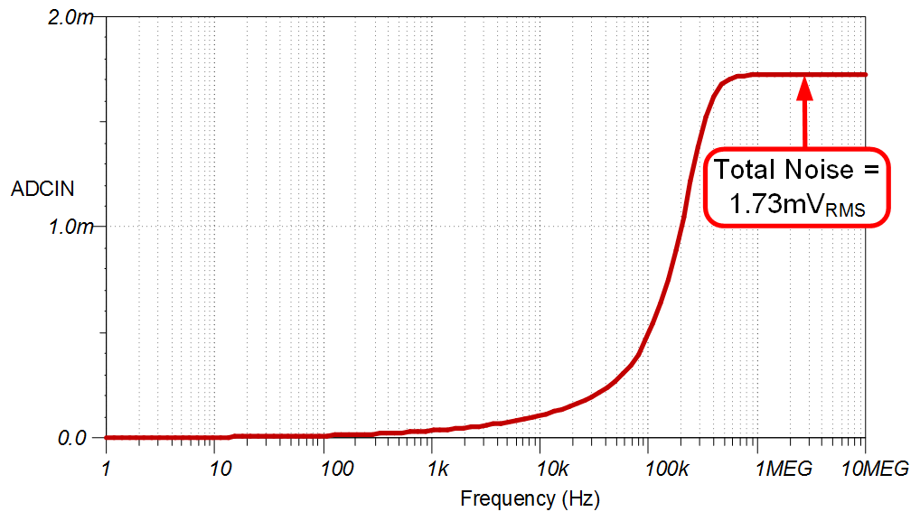
| Noise (at the input) | 1.9mVRMS | 1.73mVRMS |
| Closed-loop bandwidth | 175kHz | 185kHz |
Design Notes
- The ADS7945 was selected due to its low power and a compatible analog input structure with the ISO224.
- Verify the systems linear operation for the desired input signal range. This is verified using simulation in the DC Transfer Characteristics selection.
- Select COG capacitors for CFILT to minimize distortion.
- Understanding and Calibrating the Offset and Gain for ADC Systems covers methods for error analysis. Review the link for methods to minimize gain, offset, drift, and noise errors.
- The TI Precision Labs - ADCs training video series covers methods for selecting the charge bucket circuit RFILT and CFILT. These component values are dependent on the amplifier bandwidth, data converter sampling rate, and data converter design. The values shown here will give good settling and AC performance for the amplifier and data converter in this example. If the design is modified, a different RC filter must be selected. Refer to Introduction to SAR ADC Front-End Component Selection for an explanation of how to select the RC filter for best settling and AC performance.
Component Selection
- Select an isolated amplifier based
on the input voltage range and determine the output common-mode voltage and
output voltage range:
- ±12-V single-ended input range
- Fixed gain of ⅓, yielding ±4-V differential output
- Output common-mode voltage of +2.5V
- 4.5-V to 18-V high-side power supply, 4.5-V to 5.5-V low-side power supply
- Input Offset: ±5mV at 25°C, ±42µV/°C maximum
- Gain Error: ±0.3% at 25°C, ±50ppm/°C maximum
- Nonlinearity: ±0.01% max, ±1ppm/°C
- High-input impedance of 1.25MΩ
- Select an ADC with an appropriate
common-mode and differential input range to pair with the +2.5-V common-mode and
±4-V differential output of the ISO224:
- ±5-V maximum analog input range
- Full-scale input span set by ±voltage reference
- Input common-mode range of VREF / 2 ±0.2V
- 2.7-V to 5.25-V power supply
- High SNR of 84, low power of 11.6mW at 2Msps
- Select a voltage reference that
supports the common-mode constraint set by the 2.5-V common-mode output of the
ISO224 and the VREF / 2 ±0.2-V
common-mode input voltage of the ADS7945. This means that the reference output
voltage must be 5V, low noise, and a configurable input voltage is preferred:
- 5-V output
- 5.2-V to 18-V input voltage power supply
- 3μVPP/V noise
- Select R1FILT,
R2FILT, and CFILT for settling of the input signal and
sample rate of 100ksps:
Refine the RFILT and CFILT Values is a TI Precision Labs video showing the methodology for selecting RFILT and CFILT. The final value of 120Ω and 510pF proved to settle to well below ½ of a least significant bit (LSB) within the acquisition window.
DC Transfer Characteristics
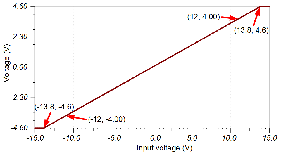
The following graph shows the simulated output for a ±15-V input. The desired linear range is a ±4-V output for a ±12-V input. This simulation shows that the linear output range is approximately ±4.6V which is well beyond the requirement.
The transfer function shows the ISO224 gain is ⅓ (that is, Gain · VIN = VOUT, (⅓)·(12V) = 4V).
AC Transfer Characteristics
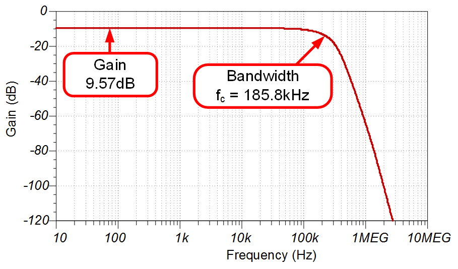
The simulated bandwidth is approximately 186kHz and the gain is –9.57dB (or 0.332V/V) which closely matches the expected gain and bandwidth for the ISO224 (specified fc = 175kHz, gain = 0.333V/V).
Transient ADC Input Settling Simulation
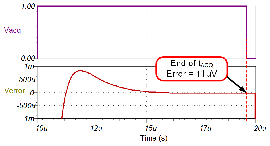
The following simulation shows the transient settling results with an acquisition time of 9.6μs. The 11-μV settling error is well within the 0.5 × LSB limit of 305μV. See Refine the Rfilt and Cfilt Values for detailed theory on this subject.
Noise Simulation
The following noise calculation looks only at the noise of the ISO224. The ISO224 noise is substantially higher than other noise sources in the circuit, so the total noise can be approximated as the ISO224 noise. The same method can be used for the B grade.
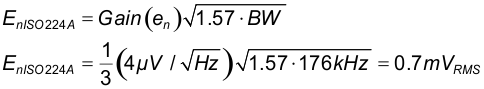
The simulated noise is greater than the expected calculated noise. This difference is due to noise peaking in the simulation model. The noise peaking is not included in the calculation. Refer to Calculating the Total Noise for ADC Systems for detailed theory on this subject.
Design Featured Devices
| Device | Key Features | Link | Similar Devices |
|---|---|---|---|
| ISO224 | ±12-V single-ended input range, Fixed gain of ⅓, yielding ±4-V differential output, output common-mode voltage of +2.5V, 4.5-V to 18-V high-side power supply, 4.5-V to 5.5-V low side power supply, input offset: ±5mV at 25°C, ±42µV/°C max, gain error: ±0.3% at 25°C, ±50ppm/°C maximum, nonlinearity: ±0.01% maximum, ±1ppm/°C, high-input impedance of 1.25MΩ | www.ti.com/product/ISO224 | www.ti.com/isoamps |
| ADS7945 |
±5 V max analog input range, full-scale input span set by ±voltage reference, input common mode range of VREF / 2 ±0.2V, 2.7-V to 5.25-V power supply, high SNR of 84, low power of 11.6mW at 2Msps |
www.ti.com/product/ADS7945 | http://www.ti.com/opamps |
| REF5050 | 3ppm/°C drift, 0.05% initial accuracy, 4μVpp/V noise | www.ti.com/product/REF5050 | http://www.ti.com/vref |
Design References
See Analog Engineer's Circuit Cookbooks for TI's comprehensive circuit library.
Link to Key Files
See the TINA files for Isolated Design.