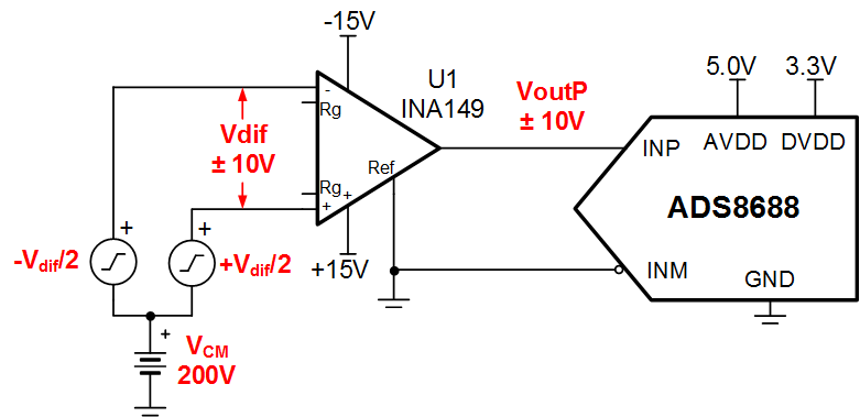
High Common-Mode Differential Input Voltage to ±10-V ADC Input Circuit
| Input | ADC Input | Digital Output ADS8688 |
|---|---|---|
| VinDiffMin = –10.24V | CH_x = –10.24V | 0000H |
| VinDiffMax = +10.24V | CH_x = +10.24V | FFFFH |
| AVDD | DVDD | AGND | DGND |
|---|---|---|---|
| 5.0V | 3.3V | GND | GND |
Design Description
The purpose of this cookbook is to demonstrate the advantages and disadvantages of using difference amplifiers or instrumentation amplifiers to translate a signal with a high common mode voltage (Vcm) to a level that the ADS86XX family can accept. The ADS86XX family cannot support a high Vcm so using a difference or instrumentation amplifier to drive the ADC solves this issue. The INA828 device is an instrumentation amplifier with very high input impedance (100GΩ), excellent DC precision, and low noise. The INA828 can accept common-mode signals in the range of its supply voltage (±15V). The INA149 device is a unity-gain difference amplifier with a high input common-mode voltage range of up to ±275V, but the input impedance is lower than the INA828 device (differential = 800kΩ, common mode = 200kΩ). The ADS86XX family of ADCs has an integrated analog front end (AFE) and multiplexer which makes it an excellent candidate for a PLC (analog input module), protection relay, grid automation, and other various industrial applications.
| Specification | Calculated | Simulated | Measured |
|---|---|---|---|
| INA149 Common-Mode Voltage (VCM) | 275V | 275V | 275V |
| INA828 Common-Mode Voltage (VCM) | 8.38V | 8.38V | 7.5V |
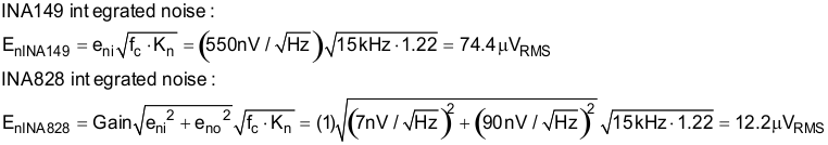
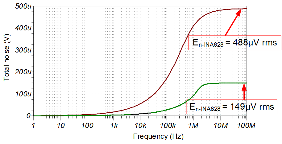
| INA149 Integrated Noise | 487µV | 487.3µV | 488µV |
| INA828 Integrated Noise | 150µV | 150µV | 154µV |
Design Notes
- The ADS86XX family of HV SAR ADCs was selected because of the integrated analog front end and multiplexer. The integrated AFE eliminates the use of extra components to drive the ADC.
- The INA149 device was selected to provide a very high common-mode voltage (Vcm = ±275V).
- Comparing the INA828 device to the INA149 shows that the INA828 device has high input impedance (100GΩ), and the INA149 device has lower input impedance (differential = 800kΩ, common mode = 200kΩ). Also, the INA149 device has very wide common mode (Vcm = ±275V) but the INA828 common mode range is limited to the supply range (for example, ±15V). In cases where high input impedance is required, the INA828 device can be used, but be careful to not violate common-mode range. Note that high input impedance is important when the sensor output impedance is high as this creates a voltage divider effect and introduce error.
- In this example, the input signal is ±10.24V. Therefore, resistor Rg is not needed to set the Gain = 1 for the INA828 device. If the input signal is smaller, use the appropriate resistor value to set the gain with a proper reference voltage on reference pin to achieve an input swing that matches the input range of the ADC.
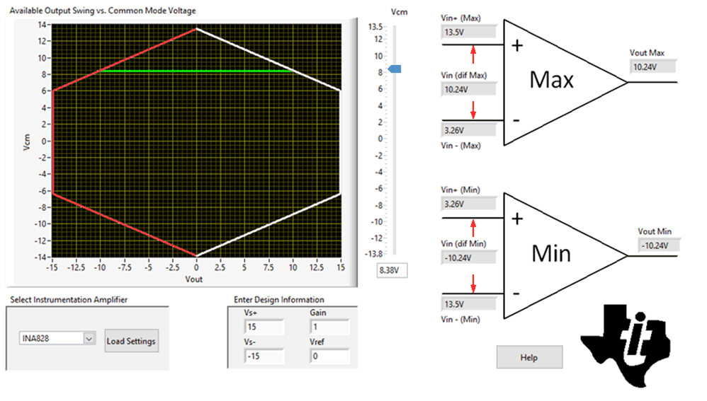
- Check the common mode range of the instrumentation amplifier using the Common-Mode Input Range Calculator for Instrumentation Amplifiers software tool.
- If gain is required, use 0.1% 20ppm/°C film resistors or better for the gain setting resistor (Rg) to achieve best gain accuracy and low gain drift.
Component Selection
- The ADS86XX can accept a single-ended input signal of ±10.24V. In this example, the input signal is ±10.24V so no external gain set resistor is required for the INA828 device. The INA149 device is a unity gain difference amplifier so no extra components are necessary.
- The INA828 reference voltage input is used to shift inputs to match the input range of the ADC. In this example, the ADC input range is symmetrical so the reference pin is grounded.
- Determine if the INA828 device is
violating the common-mode range by using the Common-Mode
Input Range Calculator for Instrumentation amplifiers. In this
example, the INA828 device shows that you can achieve a maximum VCM of 8.38V
with ±15V supplies, Gain = 1, and Vref = 0V.
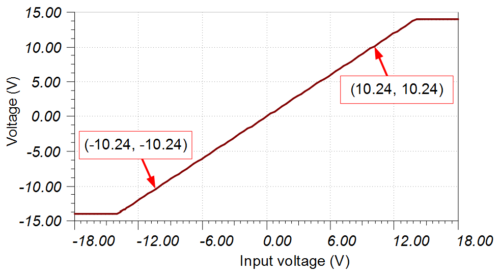
DC Transfer Characteristics
The following graphs show a linear output response for the INA149 device. The input range of the ADC is ±10.24V so the amplifier is linear well beyond the range the ADC requires. Refer to Determining a SAR ADC’s Linear Range when using instrumentation amplifiers for detailed theory on this subject.
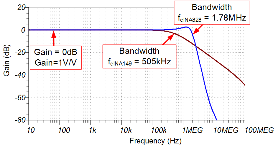
AC Transfer Characteristics
The simulated bandwidth for the INA149 device is 505kHz at gain = 1V/V, or 0dB. The simulated bandwidth for the INA828 device is 1.78MHz at a gain of 0dB. Both of the simulated bandwidths closely match the respective data sheets. See Amplifier Bandwidth Video Series for more details on this subject.
Transient ADC Input Settling Simulation
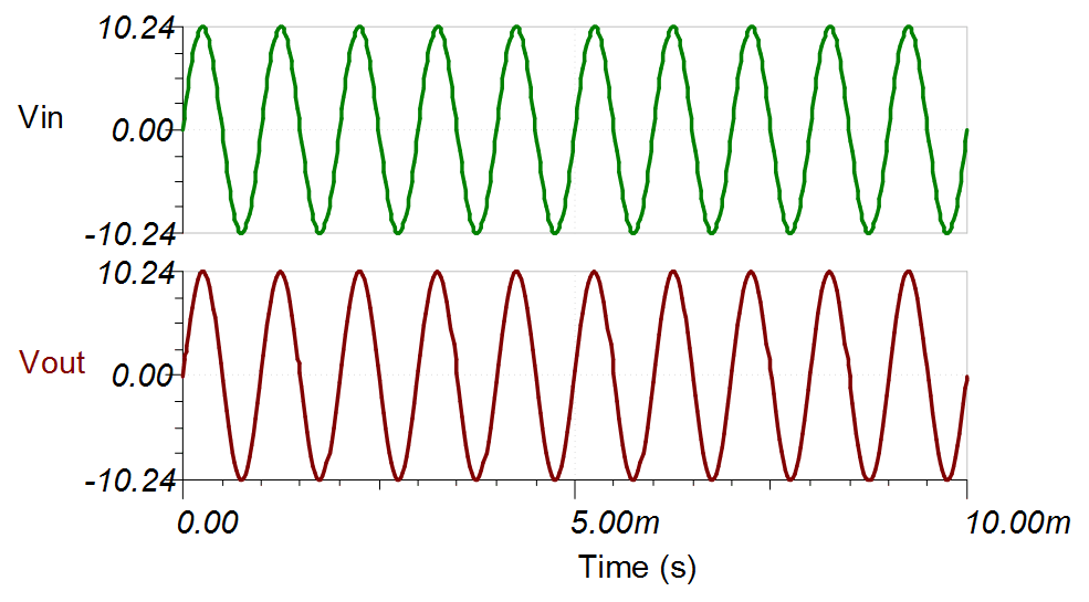
The INA149 device was simulated with a ±10.24-V differential input and a 275-V common-mode voltage. The following TINA simulation shows the differential input as well as the single-ended output for the INA149 device. The device has no issue with a common-mode voltage of 200V.
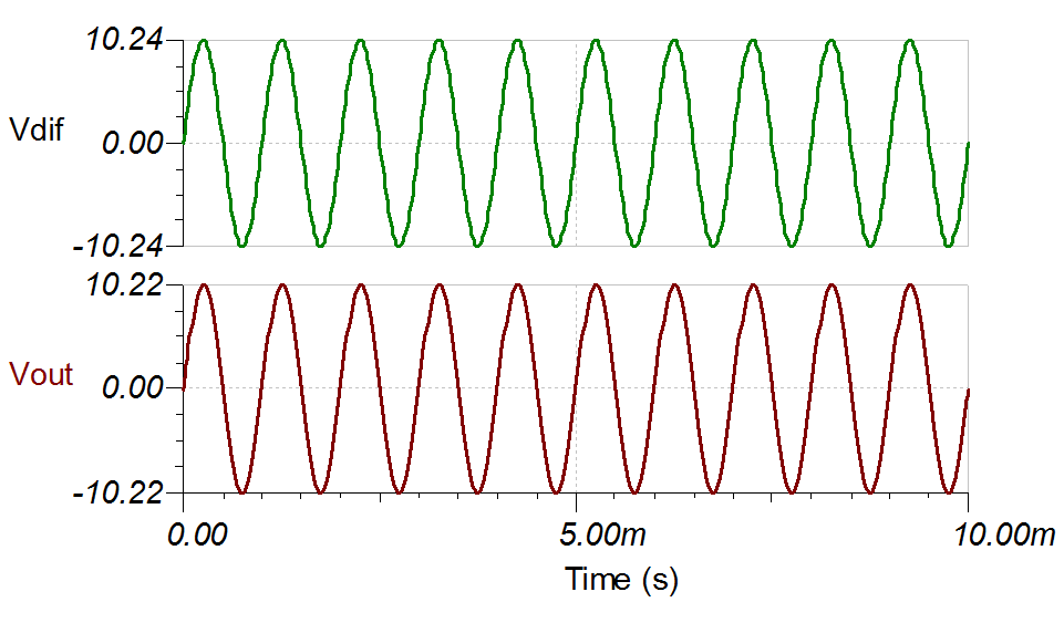
The INA828 device was simulated with a ±10.24-V differential input and a 7.75-V common-mode voltage. The following TINA simulation shows the differential input as well as the single-ended output for the INA828 device.
Noise Simulation
The section provides simplified noise calculations for the INA149 and INA828 devices. The simulated results closely match the calculated results. Refer to Op Amps: Noise 4 for detailed theory on amplifier noise calculations, and Calculating the Total Noise for ADC Systems for data converter noise.
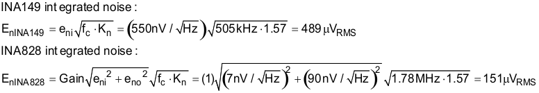
The ADS8688 device has an internal second-order 15-kHz LPF. This filter significantly reduces the noise from the instrumentation amplifiers.
Design Featured Devices
| Device | Key Features | Link | Other Possible Devices |
|---|---|---|---|
| ADS86XX | 16-Bit Resolution, 4-,8-Channel MUX, SPI, 500ksps sample rate, on-chip 4.096V Reference | 16-bit, 500-kSPS, 8-channel, single-supply SAR ADC with bipolar input ranges | Analog-to-digital converters (ADCs) |
| INA149 | 500kHz BW, Very High VCM, excellent nonlinearity | High Common Mode Voltage Difference Amplifier | Fully differential amplifiers |
| INA828 | 2MHz BW, Low Power12nV/√Hz noise | 50-μV Offset, 7-nV/√Hz Noise, Low-Power, Precision Instrumentation Amplifier | Instrumentation amplifiers |
Link to Key Files
Texas Instruments, SBAC224 source files, software support
Trademarks
All trademarks are the property of their respective owners.
IMPORTANT NOTICE AND DISCLAIMER
TI PROVIDES TECHNICAL AND RELIABILITY DATA (INCLUDING DATASHEETS), DESIGN RESOURCES (INCLUDING REFERENCE DESIGNS), APPLICATION OR OTHER DESIGN ADVICE, WEB TOOLS, SAFETY INFORMATION, AND OTHER RESOURCES “AS IS” AND WITH ALL FAULTS, AND DISCLAIMS ALL WARRANTIES, EXPRESS AND IMPLIED, INCLUDING WITHOUT LIMITATION ANY IMPLIED WARRANTIES OF MERCHANTABILITY, FITNESS FOR A PARTICULAR PURPOSE OR NON-INFRINGEMENT OF THIRD PARTY INTELLECTUAL PROPERTY RIGHTS.
These resources are intended for skilled developers designing with TI products. You are solely responsible for (1) selecting the appropriate TI products for your application, (2) designing, validating and testing your application, and (3) ensuring your application meets applicable standards, and any other safety, security, or other requirements. These resources are subject to change without notice. TI grants you permission to use these resources only for development of an application that uses the TI products described in the resource. Other reproduction and display of these resources is prohibited. No license is granted to any other TI intellectual property right or to any third party intellectual property right. TI disclaims responsibility for, and you will fully indemnify TI and its representatives against, any claims, damages, costs, losses, and liabilities arising out of your use of these resources.
TI’s products are provided subject to TI’s Terms of Sale (www.ti.com/legal/termsofsale.html) or other applicable terms available either on ti.com or provided in conjunction with such TI products. TI’s provision of these resources does not expand or otherwise alter TI’s applicable warranties or warranty disclaimers for TI products.
Mailing Address: Texas Instruments, Post Office Box 655303, Dallas, Texas 75265
Copyright © 2024, Texas Instruments Incorporated
