SBAA355A March 2019 – September 2024 ADS1118 , ADS1119 , ADS1120 , ADS112C04 , ADS112U04 , ADS1146 , ADS1147 , ADS1148 , ADS114S06 , ADS114S06B , ADS114S08 , ADS114S08B , ADS1219 , ADS1220 , ADS122C04 , ADS122U04 , ADS1246 , ADS1247 , ADS1248 , ADS124S06 , ADS124S08 , ADS125H02 , ADS1260 , ADS1261 , ADS1262 , ADS1263
| Input Measurement | ADC Input | Digital Output ADS1120 |
|---|---|---|
| T = –270°C, K-type | AINP – AINN = –6.5mV | F300H or –332810 |
| T = 1370°C, K-type | AINP – AINN = 55mV | 6E00CH or 2816010 |
| AVDD, DVDD | AVSS, DGND | |
|---|---|---|
| 3.3V | 0V | |
Design Description
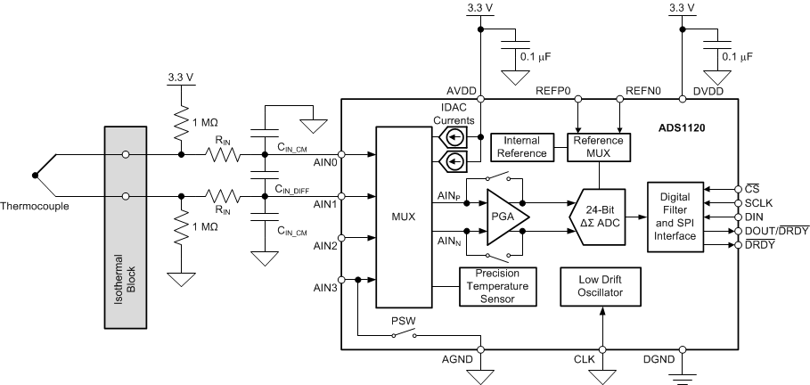
This cookbook design describes a temperature measurement for a single thermocouple using the ADS1120. The ADS1120 device then takes a separate measurement to measure the temperature of the thermocouple cold junction for cold-junction compensation (CJC). Calculations for this design are shown for a single K-type thermocouple with a temperature measurement range from –270°C to 1370°C. This circuit can be used in applications such as analog input modules for PLCs, lab instrumentation, and factory automation. For more information about making precision ADC measurements with a variety of RTD wiring configurations, see A Basic Guide to Thermocouple Measurements.

Design Notes
- Use supply decoupling capacitors for both analog and digital supplies. AVDD and DVDD must be decoupled with at least a 0.1-μF capacitor to GND. See the ADS1120 4-Channel, 2kSPS, Low-Power, 16-Bit ADC with Integrated PGA and Reference data sheet for details on power-supply recommendations.
- When possible, use C0G (NPO) ceramic capacitors for input filtering. The dielectric used in these capacitors provides the most stable electrical properties over voltage, frequency, and temperature changes. Because of size, X7R capacitors are the next best alternative.
- Cold-junction compensation is required for accurate measurement of the thermocouple temperature.
- The K-type thermocouple has a large input range and thermocouple voltage. Other thermocouples have different sensitivities and error tolerances. For measurements with other thermocouples and a guide to use them, see A Basic Guide to Thermocouple Measurements.
- Conversion tables and polynomial equations used to determine thermocouple temperature from the thermoelectric voltage are found in the NIST Temperature Scale Database. Additionally, the Analog engineer's calculator determines some thermocouple conversions.
Component Selection
- Identify the range of operation for the thermocouple.
The K-type thermocouple has a range of approximately −6.5mV to +55mV, if the temperature measurement range is from −270°C to 1370°C. This range is used to maximize the resolution of the measurement, considering the full-scale range of the ADC.
- Determine gain and input range of the ADC.
Calculate the maximum gain allowed without over-ranging the programmable gain amplifier (PGA) based on the maximum thermocouple output voltage and the reference voltage. Then establish that the thermocouple biasing is near mid-supply so that the input signal is in the common-mode input range of the PGA.
For the ADS1120 device, the PGA can amplify the input signal from gains of 1 to 128 in factors of 2. With an input range of −6.5mV to +55mV, the maximum gain used is 32 without over-ranging the PGA using the internal reference voltage of 2.048V.
% of usable ADC range = 32 × [55mV – (–6.5mV)] ÷ [2.048V – (–2.048V)] × 100% = 48.0%Number of ADC codes in measurement range = 0.48 × 216 = 31488With the temperature range of −270°C to 1370°C for the thermocouple, 31488 codes are used to represent a range of 1640°C. This equates to approximately 0.052°C per ADC code.
- Set up the resistor biasing to establish the input DC level and
burn-out detection.
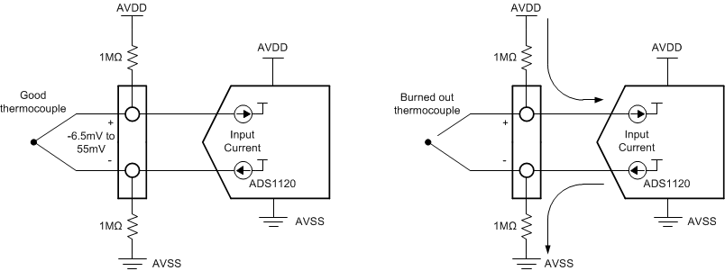
Equal biasing resistors are tied from either end of the thermocouple to AVSS and AVDD. In normal operation, the resistors set the DC biasing point of the thermocouple to near mid-supply. If the thermocouple burns out and becomes an open circuit, the resistors pull apart the thermocouple leads to either supply. These resistors are set high (often 500kΩ to 10MΩ) to reduce the bias current going through the thermocouple. Resistor bias current reacting with the thermocouple lead resistance causes measurement error. However, the resistors must also be low enough to provide sufficient bias current to overcome any input current from the resistor.
In this design, biasing resistors are chosen to be 1MΩ. This value sets the resistor biasing current to a low 1.65μA (assuming the resistors bias the thermocouple at center of the 3.3-V supply). However, in the case of a burned out thermocouple, 1MΩ provides more than enough current to separate the ADC inputs against any input current of the ADC.

In the case of the good thermocouple, the thermocouple voltage has a range of –6.5mV to 55mV. The remaining 3.3V of the VDD supply is dropped equally between the biasing resistors. With 1-MΩ bias resistors, the thermocouple voltage has a DC operating point near mid-supply at 1.65V.
In the case of a burned out thermocouple, the 1-MΩ bias resistors overcome the input current to pull apart the input voltage so that the ADC reads a full-scale input reading. Based on the typical characteristics curves, the absolute input current is 250nA depending upon temperature, input voltage, and input channel. Assuming this input current at each input, the input current drops the same voltage across the two bias resistors:
ADC input voltage = 3.3V – (1MΩ × 250nA) – (1MΩ × 250nA) = 2.8VIf the thermocouple burns out, the ADC input voltage is 2.8V, which is much larger that the positive full-scale reading of the ADC. The ADC reports a reading of 7FFFh to indicate a burn-out condition. Note that this assumes the largest input current. With lower operating temperature or different inputs, the ADC input can be larger.
- Select values for the differential and common-mode input
filtering for the ADC inputs and reference inputs.
If there is input filtering, the input current reacts with any series filter resistance to create an error. For this reason, the input series resistance is kept low to reduce any possible error.
This design includes differential and common-mode input RC filtering. The bandwidth of the differential input filtering is set to be at least 10 × higher than the data rate of the ADC. The common-mode capacitors are selected to be 1/10 of the value the differential capacitor. Because of capacitor selection, the bandwidth of common-mode input filtering is approximately 20 × higher than the differential input filtering.
With input filtering, differential signals are attenuated at a lower frequency than the common-mode signals, which are significantly rejected by the PGA of the device. Mismatches in common-mode capacitors cause an asymmetric noise attenuation, appearing as a differential input noise. With a lower bandwidth for differential signals, the effects from the mismatch of input common-mode capacitors are reduced. Input filtering for the ADC inputs and reference inputs are designed for the same bandwidth.
In this design, the data rate is chosen to be 20SPS. For the ADC input filtering, the bandwidth frequency for the differential and common-mode filtering is approximated in the following equations:
fIN_DIFF = 1 ÷ (2 × π × CIN_DIFF × 2 × RIN)fIN_CM = 1 ÷ (2 × π × CIN_CM × RIN)For the ADC input filtering, RIN = 800Ω, CIN_DIFF = 0.47µF, and CIN_CM = 0.047µF. This sets the differential filter bandwidth to 330Hz and the common-mode filter bandwidth to 4.2kHz.
- Use cold-junction compensation to
calculate the actual thermocouple voltage based on the cold-junction
temperature.
To get a precise measurement from a thermocouple, cold-junction compensation must be performed to get an accurate temperature measurement. An accurate measurement of the cold-junction where the thermocouple leads are tied is required. You cannot simply add the temperature of the cold-junction to the temperature computed from the thermocouple voltage. To accurately determine the thermocouple temperature, the proper method is to:
- Convert the cold-junction temperature (TCJ) to a voltage (VCJ)
- Add the cold-junction voltage to the measured thermocouple voltage (VCJ + VTC)
- Convert the summed cold-junction voltage and thermocouple voltage to the thermocouple temperature (TTC)
The following flow diagram shows the conversion method to determine the actual temperature of the thermocouple based on the ADC measurements.

Conversion tables and polynomial equations used to determine thermocouple temperature from the thermoelectric voltage are found at the NIST website: http://srdata.nist.gov/its90/menu/menu.html.
Because the ADS1120 device has an accurate internal temperature sensor, a measurement can be used. The internal temperature sensor has a typical accuracy of 0.25°C for a range of 0°C to 75°C. This accuracy is best for the cold-junction measurement. However, the device requires a good thermal contact to the connection for the thermocouple cold-junction. Any error in the cold-junction measurement yields an error in the resulting temperature measurement. Note that the ADS1120 device does not specify a maximum error for the temperature sensor.
For more information about thermocouples and the cold-junction compensation measurement, see A Basic Guide to Thermocouple Measurements.
- Cold-junction compensation can be made through alternate
methods.
Use alternate cold-junction measurements because the ADS1120 device has an additional analog input channel, internal voltage reference, and an external reference input.
As an example, while AIN0 and AIN1 are used for the thermocouple, use AIN2 and AIN3 to measure an RTD. This would require a reference resistor and a connection to the external reference inputs. The ADS1120 device has current IDAC sources that can be used for excitation of the RTD and reference resistor. Alternately, use AIN2 and AIN3 to measure other temperature sensors like the LMT70. The LMT70 precision analog temperature sensor outputs a voltage based on the ambient temperature of the device.
For more information about RTDs, see A Basic Guide to RTD Measurements. For more information about the LMT70, see the LMT70, LMT70A ±0.05°C Precision Analog Temperature Sensor, RTD and Precision NTC Thermistor IC data sheet.
- An extra input channel and other
ADS1120 features are available for other measurements.
The circuit schematic is drawn with AIN2 and AIN3 unused and can be used for other measurements.
If the device cannot be placed at the cold-junction temperature, an alternate cold-junction measurement must be made. As mentioned in the previous section, AIN2 and AIN3 can be used with the external reference to make an RTD measurement if the internal temperature sensor is not used. Enable IDAC current sources in the ADS1120 device for excitation of the RTD and the reference resistor. However, in this design, the configuration register and pseudocode are set when the internal temperature sensor is enabled, and the IDACs are disabled.
Additionally, AIN3 is internally connected to a low-side power switch (PSW). Use the low-side PSW in resistive bridge applications to disconnect a bridge when not in use, reducing the current consumption. For this circuit, the PSW is unused in this design and disabled.
The ADS1120 device has a set of burn-out current sources (BCS) which can be used enable current sources at the ADC inputs to pull apart the input voltage when the thermocouple is burned out. In this design, the bias resistors serve the same purpose and the BCS is disabled. However, if the thermocouple is biased from a voltage, without biasing resistors, the BCS can be necessary for burnout detection.
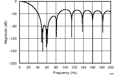
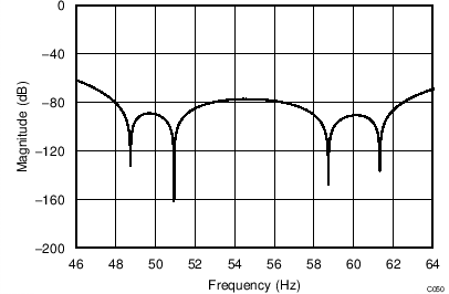
The ADS1120 device uses a finite impulse response digital filter that can be configured for different data rates and different frequency responses. At data rates of 5SPS and 20SPS, the filter can be configured to reject 50-Hz or 60-Hz line frequencies or to simultaneously reject 50 Hz and 60 Hz. Two bits (50/60[1:0]) in the configuration register are used to configure the filter accordingly. At 20SPS, the digital filter frequency responses are shown. The 50/60[1:0] bits are enabled in this design.
For more information about features in the ADS1120 device, see the ADS1120 4-Channel, 2-kSPS, Low-Power, 16-Bit ADC with Integrated PGA and Reference data sheet.

Simultaneous
50-Hz and 60-Hz rejection, 50/60[1:0] = 01
Filter
Response (DR = 20SPS) |

Simultaneous
50-Hz and 60-Hz rejection, 50/60[1:0] = 01
Detailed View
of Filter Response (DR = 20SPS) |
Measurement Conversion
Conversions for the thermocouple voltage are relatively straightforward based on the full-scale range setting of the ADC.
Measurement 1 (Thermocouple):
If the internal temperature sensor is used, conversions for the internal temperature sensor require some data manipulation. Temperature data from the ADC are represented as a 14-bit result that is left-justified within the 16-bit conversion result. Data are output starting with the most significant byte (MSB). When reading the two data bytes, the first 14 bits are used to indicate the temperature measurement result. One 14-bit LSB equals 0.03125°C and negative numbers are represented in binary twos complement format.
Measurement 2 (Internal Temperature Sensor):
OutputCode2 is the first 14 bits of the two-byte output data from the ADC.
Register Settings
Measurement 1 (Thermocouple):
| Bit | Field | Setting | Description |
|---|---|---|---|
| 7:4 | MUX[3:0] | 0000 | AINP is AIN0 and AINN is AIN1 for thermocouple measurement |
| 3:1 | GAIN[2:0] | 101 | Gain = 32 |
| 0 | PGA_BYPASS | 0 | PGA enabled |
| Bit | Field | Setting | Description |
|---|---|---|---|
| 7:5 | DR[2:0] | 000 | Data rate = 20SPS |
| 4:3 | MODE[1:0] | 00 | Normal mode |
| 2 | CM | 0 | Single-shot conversion mode |
| 1 | TS | 0 | Temperature sensor disabled |
| 0 | BCS | 0 | Burn-out current sources off |
| Bit | Field | Setting | Description |
|---|---|---|---|
| 7:6 | VREF[2:0] | 00 | Internal 2.048V reference selected |
| 5:4 | 50/60[1:0] | 01 | Simultaneous 50-Hz and 60-Hz rejection enabled |
| 3 | PSW | 0 | Switch is always open (used in bridge applications) |
| 2:0 | IDAC[2:0] | 000 | IDAC current sources off |
| Bit | Field | Setting | Description |
|---|---|---|---|
| 7:5 | IMUX1[2:0] | 000 | IDAC1 disabled |
| 4:2 | IMUX2[2:0] | 000 | IDAC2 disabled |
| 1 | DRDYM | 0 | Only the dedicated DRDY pin is used to indicate when data are ready |
| 0 | Reserved | 0 | Always write 0 |
Measurement 2 (Internal Temperature Sensor):
| Bit | Field | Setting | Description |
|---|---|---|---|
| 7:5 | DR[2:0] | 000 | Data rate = 20SPS |
| 4:3 | MODE[1:0] | 00 | Normal mode |
| 2 | CM | 0 | Single-shot conversion mode |
| 1 | TS | 1 | Temperature sensor enabled, bypasses PGA and sets the gain to 1 |
| 0 | BCS | 0 | Burn-out current sources off |
Pseudo Code Example
The following shows a pseudo code sequence with the required steps to set up the device and the microcontroller that interfaces to the ADC to take subsequent readings from the ADS1120 in single-shot conversion mode:
Configure microcontroller for SPI mode 1 (CPOL = 0, CPHA = 1)
Set CS low;
Send 43h; //WREG starting at register 00h, four bytes
0Ah 00h 10h 00h; // Register 0: AINP=AIN0, AINN=AIN1, PGA=32, PGA enabled
// Register 1: DR=20SPS, Normal mode, Single shot conversion, Temp sensor and BCS disabled
// Register 2: Internal 2.048V ref, 50Hz/60Hz rejection enabled, PSW and IDACs disabled
// Register 3: IDAC disabled, Only /DRDY pin indicates when data are ready
Set CS high;
Loop
{
Set CS low;
Send 44h; //WREG starting at register 01h, one byte
00h; // Register 1: Data Rate=20SPS, Normal mode, Single shot conversion,
// Temp sensor and BCS disabled
Set CS high;
Set CS low;
Send 08h; // Send START/SYNC command to start conversion
Set CS high;
Wait 51 ms for /DRDY to go low; // At 20SPS data rate, nominally 50ms ±2% accuracy
Set CS low;
Send 10h; // RDATA command to read data for thermocouple
 00h 00h; // Clock out 16 bits of data
Set CS high;
Set CS low;
Send 44h; //WREG starting at register 01h, one byte
02h; // Register 1: Enable temperature sensor
Set CS high;
Set CS low;
Send 08h; // Send START/SYNC command to start conversion
Set CS high;
Wait 51ms for /DRDY to go low; // At 20SPS data rate, nominally 50ms ±2% accuracy
Set CS low;
Send 10h; // RDATA command to read data for thermocouple
 00h 00h; // Clock out 16 bits of data
Set CS high;
Convert thermocouple ADC data to voltage; // Cold junction compensation to determine
// thermocouple temperature
Convert ADC temp sensor data to temperature;
Convert ADC temp sensor data to thermoelectric voltage; // By lookup table or calculation
Add thermocouple voltage to temperature thermoelectric voltage;
Convert resulting voltage for thermocouple to temperature; // By lookup table or calculation
}
Design Featured Devices
| Device | Key Features | Link | Other Possible Devices |
|---|---|---|---|
| ADS1120 | ADS1120 4-channel, 2kSPS, low-power, 16-bit ADC with integrated PGA and reference | 16-bit, 2kSPS, 4ch, low-power, small-size delta-sigma ADC with PGA, VREF, 2x IDACs and SPI interface | Precision ADCs |
Additional Resources
- Texas Instruments, ADS1120 evaluation module, software tool
- Texas Instruments, ADS1x20EVM, user's guide
- Texas Instruments, ADS1x20 Example Code, SBAC227 tool
- Texas Instruments, A Basic Guide to Thermocouple Measurements, application note
- Texas Instruments, A Basic Guide to RTD Measurements, application note