SBAK021 December 2024 AFE7950-SP
3 Device and Test Board Information
The AFE7950-SP is packaged in a 400-pin FCBGA (TI package code ALK) organic substrate flip-chip package. AFE7950EVM evaluation boards were re-worked with AFE7950-SP devices to evaluate the performance and characteristics of the AFE7950-SP under heavy-ions.
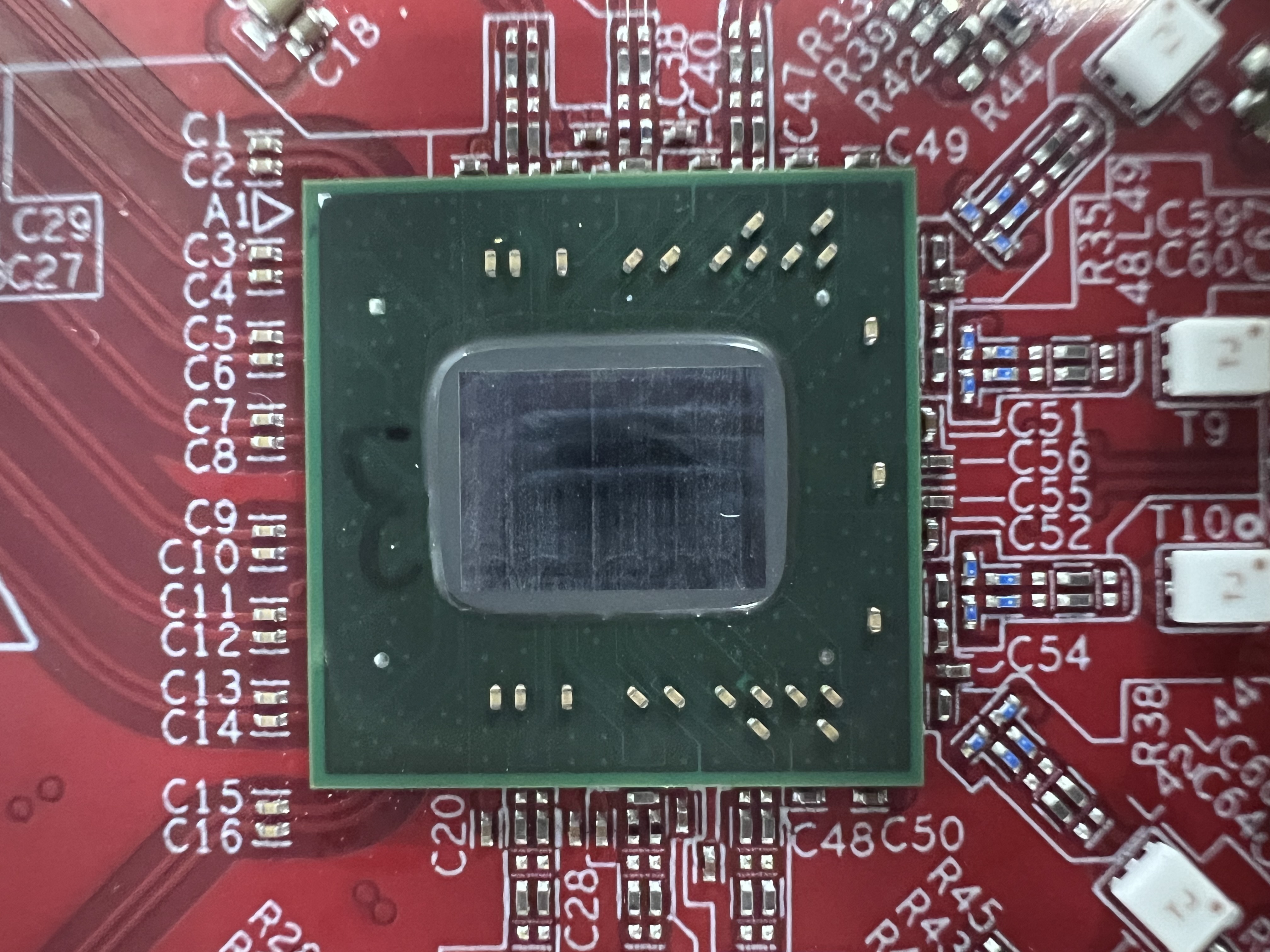
Figure 3-2 shows the top view of the evaluation board used for the radiation testing. AFE7950EVM User's Guide provides more detail on the EVM which was used for testing.
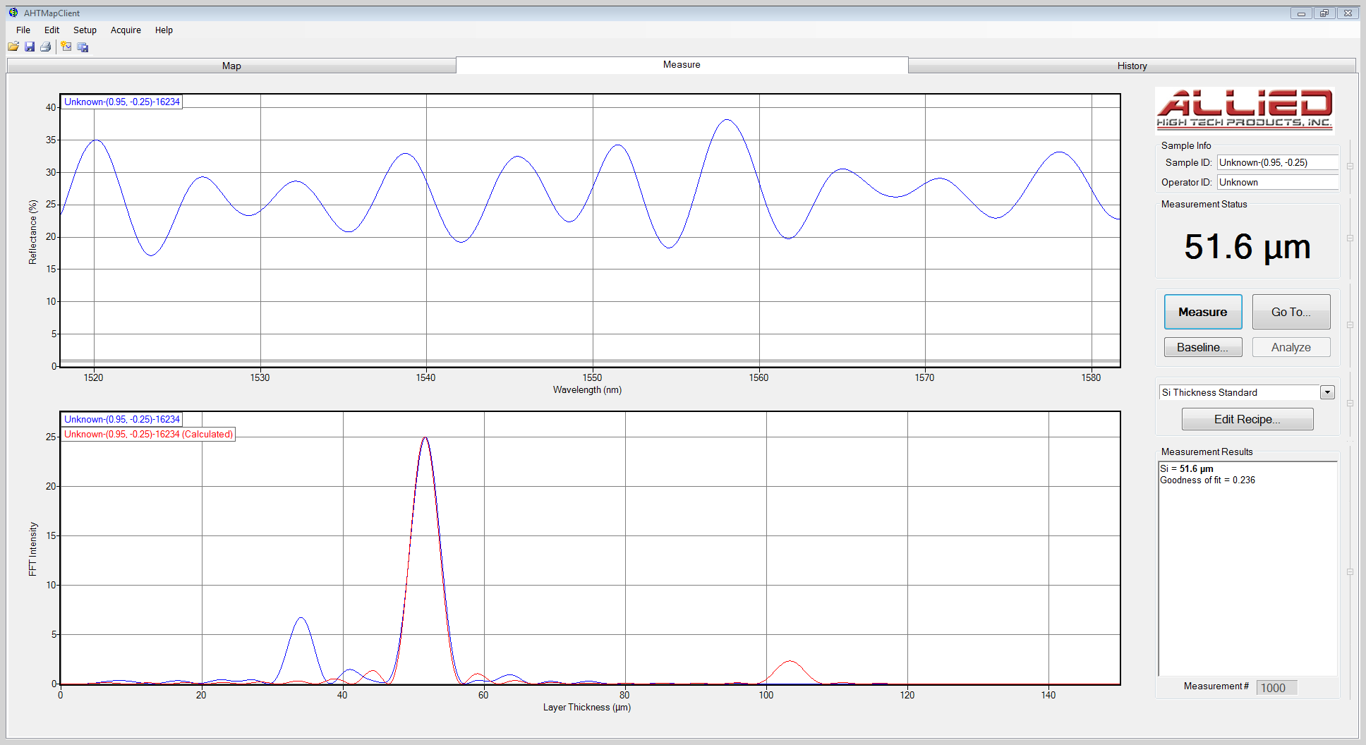
Devices are prepared by de-lidding and then thinning down the backside of silicon substrate down to target thickness of approximately 50um. Example thickness profile is shown in Figure 3-1.
 Figure 3-1 Silicon Thickness
Profile
 Figure 3-2 Photograph of Delidded
AFE7950-SP