SBASAK4B March 2023 – April 2024 ADS127L21
PRODUCTION DATA
- 1
- 1 Features
- 2 Applications
- 3 Description
- 4 Pin Configuration and Functions
-
5 Specifications
- 5.1 Absolute Maximum Ratings
- 5.2 ESD Ratings
- 5.3 Recommended Operating Conditions
- 5.4 Thermal Information
- 5.5 Electrical Characteristics
- 5.6 Timing Requirements (1.65 V ≤ IOVDD ≤ 2 V)
- 5.7 Switching Characteristics (1.65 V ≤ IOVDD ≤ 2 V)
- 5.8 Timing Requirements (2 V < IOVDD ≤ 5.5 V)
- 5.9 Switching Characteristics (2 V < IOVDD ≤ 5.5 V)
- 5.10 Timing Diagrams
- 5.11 Typical Characteristics
-
6 Parameter Measurement Information
- 6.1 Offset Error Measurement
- 6.2 Offset Drift Measurement
- 6.3 Gain Error Measurement
- 6.4 Gain Drift Measurement
- 6.5 NMRR Measurement
- 6.6 CMRR Measurement
- 6.7 PSRR Measurement
- 6.8 SNR Measurement
- 6.9 INL Error Measurement
- 6.10 THD Measurement
- 6.11 IMD Measurement
- 6.12 SFDR Measurement
- 6.13 Noise Performance
-
7 Detailed Description
- 7.1 Overview
- 7.2 Functional Block Diagram
- 7.3 Feature Description
- 7.4 Device Functional Modes
- 7.5
Programming
- 7.5.1
Serial Interface (SPI)
- 7.5.1.1 Chip Select (CS)
- 7.5.1.2 Serial Clock (SCLK)
- 7.5.1.3 Serial Data Input (SDI)
- 7.5.1.4 Serial Data Output/Data Ready (SDO/DRDY)
- 7.5.1.5 SPI Frame
- 7.5.1.6 Full-Duplex Operation
- 7.5.1.7 Device Commands
- 7.5.1.8 Read Conversion Data
- 7.5.1.9 Daisy-Chain Operation
- 7.5.1.10 3-Wire SPI Mode
- 7.5.1.11 SPI CRC
- 7.5.2 Register Memory CRC
- 7.5.1
Serial Interface (SPI)
- 8 Register Map
- 9 Application and Implementation
- 10Device and Documentation Support
- 11Revision History
- 12Mechanical, Packaging, and Orderable Information
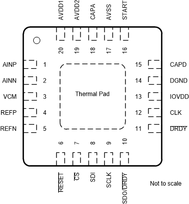
4 Pin Configuration and Functions
 Figure 4-1 RUK
Package,20-Pin WQFN(Top View)
Figure 4-1 RUK
Package,20-Pin WQFN(Top View)Table 4-1 Pin Functions
| NAME | PIN NO. | TYPE | DESCRIPTION |
|---|---|---|---|
| AINN | 2 | Analog input | Negative analog input; see the Analog Input section for details. |
| AINP | 1 | Analog input | Positive analog input; see the Analog Input section for details. |
| AVDD1 | 20 | Analog Supply | Positive analog supply 1; see the Power Supplies section for details. |
| AVDD2 | 19 | Analog Supply | Positive analog supply 2; see the Power Supplies section for details. |
| AVSS | 17 | Analog Supply | Negative analog supply; see the Power Supplies section for details. |
| CAPA | 18 | Analog output | Analog voltage regulator output capacitor bypass. |
| CAPD | 15 | Analog output | Digital voltage regulator output capacitor bypass. |
| CLK | 12 | Digital input | Clock input; see the Clock Operation section for details. |
| CS | 7 | Digital input | Chip select, active low; see the Chip Select section for details. |
| DGND | 14 | Ground | Digital ground. |
| DRDY | 11 | Digital output | Data ready, active low; see the Data Ready section for details. |
| IOVDD | 13 | Digital Supply | I/O supply voltage; see the Power Supplies section for details. |
| REFN | 5 | Analog input | Negative reference input; see the Reference Voltage section for details. |
| REFP | 4 | Analog input | Positive reference input; see the Reference Voltage section for details. |
| RESET | 6 | Digital input | Reset, active low; see the Reset section for details. |
| SCLK | 9 | Digital input | Serial data clock; see the Serial Clock section for details. |
| SDI | 8 | Digital input | Serial data input; see the Serial Data Input section for details. |
| SDO/DRDY | 10 | Digital output | Serial data output and data ready (optional); see the SDO/DRDY section for details. |
| START | 16 | Digital input | Conversion start; see the Synchronization section for details. |
| VCM | 3 | Analog output | Common-mode voltage output; see the VCM Output Voltage section for details. |
| Thermal Pad | Pad | — | Thermal power pad; connect to AVSS. |