SBAU193E June   2011  – May 2021 ADS8568


  1.   Trademarks
  2. 1EVM Overview
    1. 1.1 ADS8568EVM-PDK Kit Features
    2. 1.2 ADS8568EVM Board Features
    3. 1.3 Related Documentation From Texas Instruments
  3. 2EVM Analog Interface
    1. 2.1 ADC Supply, Input, Voltage Reference, and Digital Connections
    2. 2.2 ADC Amplifier Drive
  4. 3Digital Interface
    1. 3.1 Parallel Interface
    2. 3.2 Serial Interface (SPI)
    3. 3.3 Connections to PHI connector
    4. 3.4 Static Signals for ADS8568
    5. 3.5 I2C Bus for Onboard EEPROM
  5. 4Power Supplies
    1. 4.1 Low Dropout Regulator
    2. 4.2 Power Connections and LED Indicators
  6. 5Installing ADS8568EVM Software
  7. 6ADS8568EVM Operation
    1. 6.1 Connecting the Hardware and Running the GUI
    2. 6.2 Jumper Settings for ADS8568EVM
    3. 6.3 EVM GUI Global Settings for ADC Control
    4. 6.4 Time Domain Display
    5. 6.5 Frequency Domain Display
    6. 6.6 Histogram Display
  8. 7Modifying Hardware and Using Software to Evaluate ADS8548 and ADS8528
  9.   A Bill of Materials, Layout, and Schematic
    1.     A.1 Bill of Materials
    2.     A.2 Layout
    3.     A.3 Schematic
  10.   B Revision History

Time Domain Display

The time domain display tool allows visualization of the ADC response to a given input signal. This tool is useful for both studying the behavior and debugging any gross problems with the ADC or drive circuits.

The user can trigger a capture of the data of the selected number of samples from the ADS8568EVM, as per the current interface mode settings indicated in Figure 6-4 by using the Capture button. The sample indices are on the x-axis and there are two y-axes showing the corresponding output codes as well as the equivalent analog voltages based on the specified reference voltage. Switching pages to any of the Analysis tools described in the subsequent sections causes calculations to be performed on the same set of data.
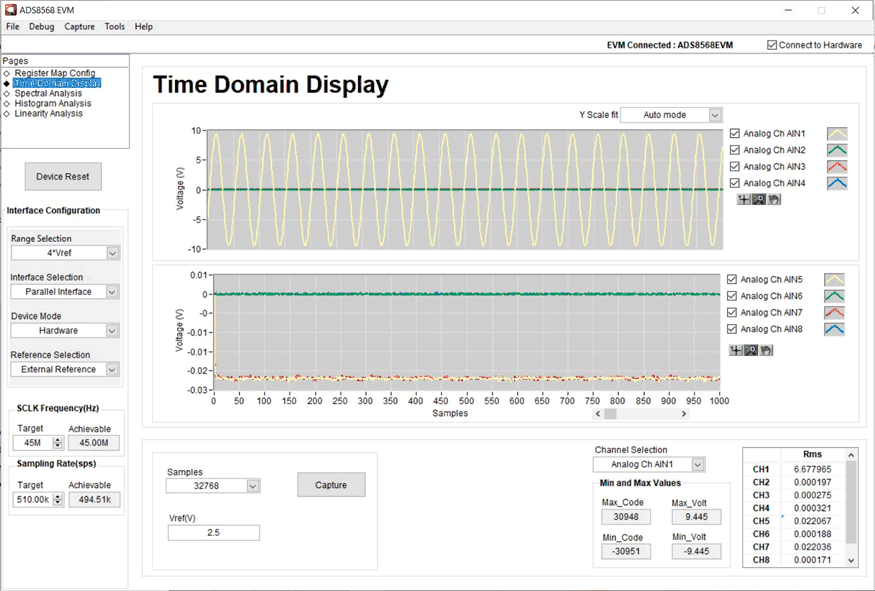
GUID-20200707-SS0I-LF5M-3XGX-5HBQ2DDXPM9D-low.gif Figure 6-4 Time Domain Display