SBAU227A March 2014 – June 2021 TPS56520 , TPS56720 , TPS56920 , TPS56C20
5.1 Board Layout
Figure 5-1 through Figure 5-5 show the board layout for the TPS56C20EVM-614. The top layer contains the main power traces for PVIN, VIN, VOUT, SWITCH node, and a huge area filled with ground. Many of the signal traces are also located on the top side. The design locates the input decoupling capacitors and the voltage set point resistor divider network components as close to the IC as possible. The input and output connectors, test points, and most of the components are located on the top side. The analog ground (which is used as a return for the I2C interface signals) connects to the power ground at only one point on the top layer. Internal layer 1 and internal layer 2 are filled with power ground. The bottom layer contains a few traces like the I2C connections and the output voltage trace to the J3 connector.
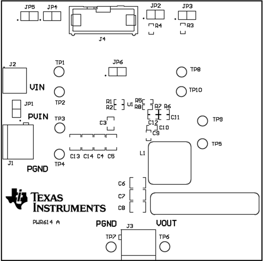 Figure 5-1 Top Assembly
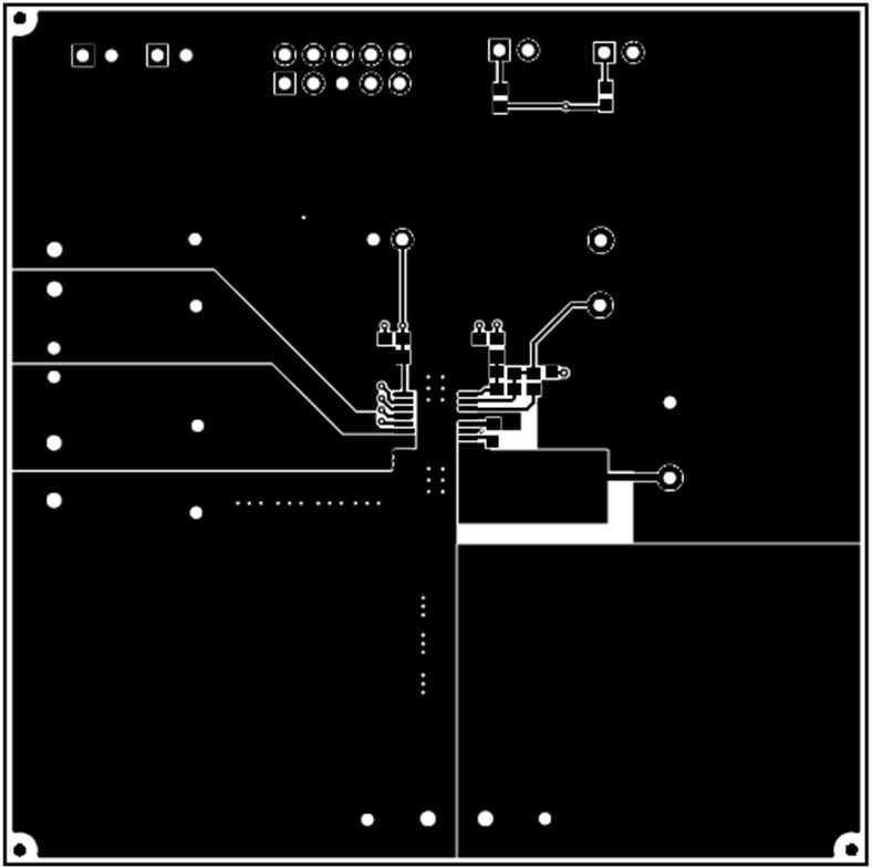 Figure 5-2 Top Layer
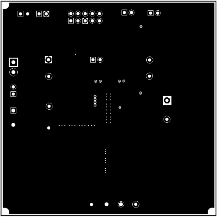 Figure 5-3 Internal Layer 1
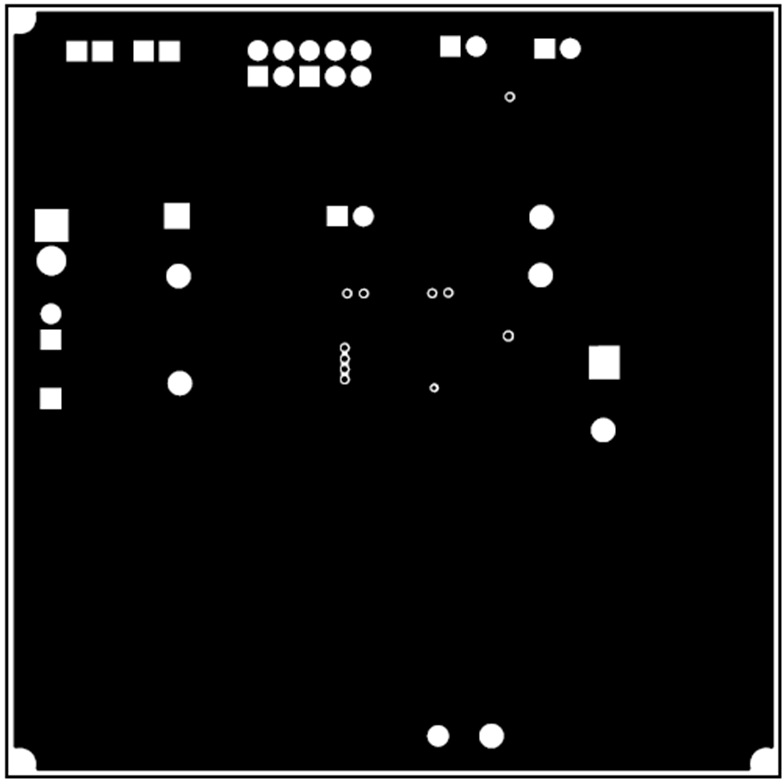 Figure 5-4 Internal Layer 2
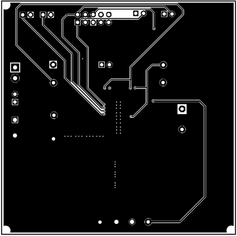 Figure 5-5 Bottom Layer