SBAU374A May 2021 – May 2022 DAC12DL3200
- Abstract
- Trademarks
- 1Introduction
- 2Equipment
-
3Setup Procedure
- 3.1 Install the High Speed Data Converter (HSDC) Pro Software
- 3.2 Install the Configuration GUI Software
- 3.3 Connect the DAC12DL3200EVM and TSW14DL3200EVM
- 3.4 Connect the Power Supplies to the Boards (Power Off)
- 3.5 Connect the Signal Generators to the EVM (*RF Outputs Disabled Until Directed)
- 3.6 Turn On the TSW14DL3200EVM 12-V Power and Connect to the PC
- 3.7 Turn On the DAC12DL3200EVM 5-V Power Supply and Connect to the PC
- 3.8 Turn On the Signal Generator RF Outputs
- 3.9 Open the DAC12DL3200EVM GUI and Program the DAC and Clocks for Single Channel, NRZ Mode 2 Operation
- 3.10 Open the HSDC Software and Load the FPGA Image to the TSW14DL3200EVM
- 3.11 DxSTRB Timing Adjustment
- 4Other Modes of Operation
- 5Register Log File
- 6Device Configuration
- A Troubleshooting the DAC12DL3200EVM
- B DAC12DL3200EVM Onboard Clocking Configuration
3.10 Open the HSDC Software and Load the FPGA Image to the TSW14DL3200EVM
Use the following steps to open the HSDC software and load the FPGA image to the TSW14DL3200EVM:
- Open the HSDC Pro software.
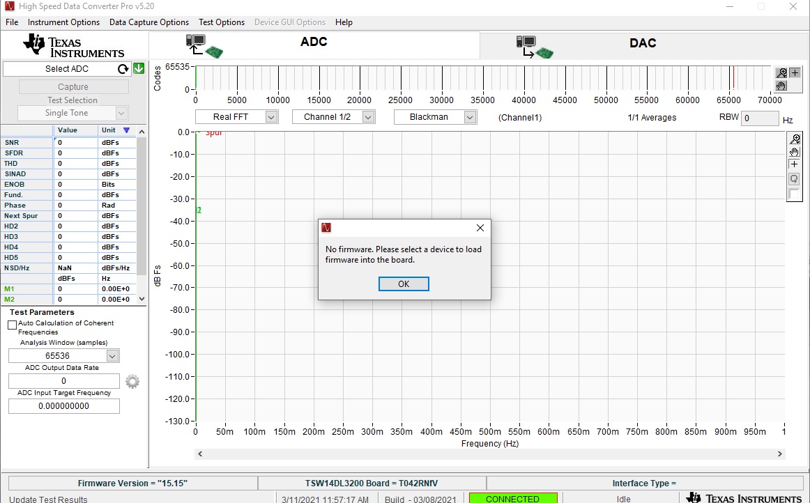
Click OK to confirm the serial number of the TSW14DL3200EVM device. If multiple TSWxxxxx boards are connected, select the model and serial number for the one connected to the DAC12DL3200EVM. When the EVM powers up, there is no firmware loaded in the FPGA. Click the OK button on the No firmware. Please select a device to load firmware into the board. message.
 Figure 3-5 No Firmware
Loaded
 - Click on the DAC tab in the
top right of the GUI.
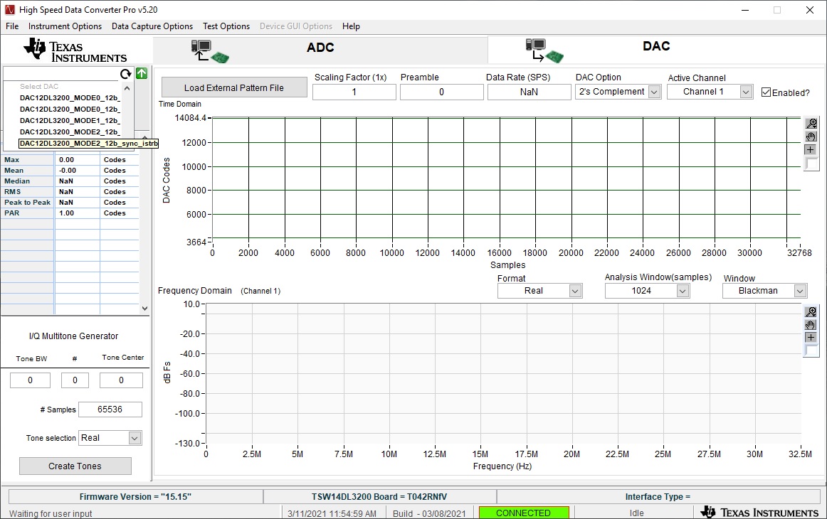
In the device drop-down menu, select "DAC12DL3200_MODE2_12b_sync_istrb” as illustrated in Figure 3-6.
 Figure 3-6 Selecting DAC Mode
2
 - When prompted, click Yes to update the firmware. After the firmware is downloaded, the configuration done LED D22 illuminates on the TSW14DL3200EVM. This is located next to the FPGA. Status LEDs D1–D5 also illuminate.
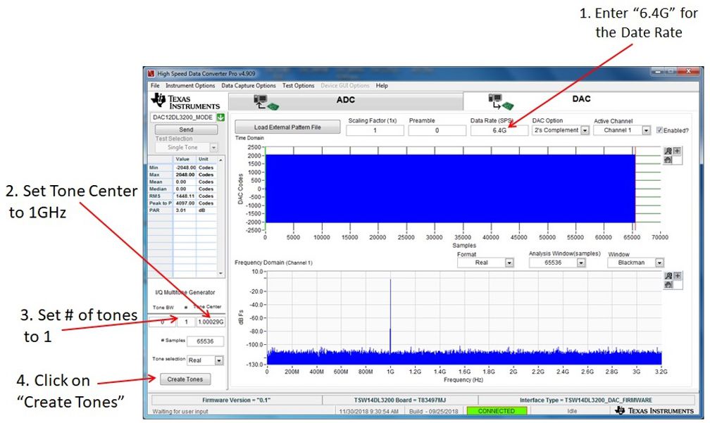
- In the top middle of the GUI, enter "6.4G" for the Data Rate.
- Set the tone center "1GHz" in the I/Q Multitone Generator window in the lower left of the GUI, .
- Enter the # of tones "1", also in the I/Q Multitone Generator window
- Click the Create Tones button.
The setup looks as shown in Figure 3-7.
 Figure 3-7 HSDC Pro GUI Setup