SBAU394A April 2022 – September 2022
- ADS1285 Evaluation Module
- Trademarks
- 1 EVM Overview
- 2 ADS1285EVM-PDK Quick-Start Guide
- 3 EVM Analog Interface
- 4 Digital Interface
- 5 Power Supplies
- 6 Digital-to-Analog Converter
- 7 ADS1285EVM-PDK Initial Setup
- 8 ADS1285EVM-PDK Software Reference
- 9 ADS1285EVM-PDK Bill of Materials, PCB Layout, and Schematics
- 10References
- 11Revision History
3.1 ADC Analog Input Signal Path
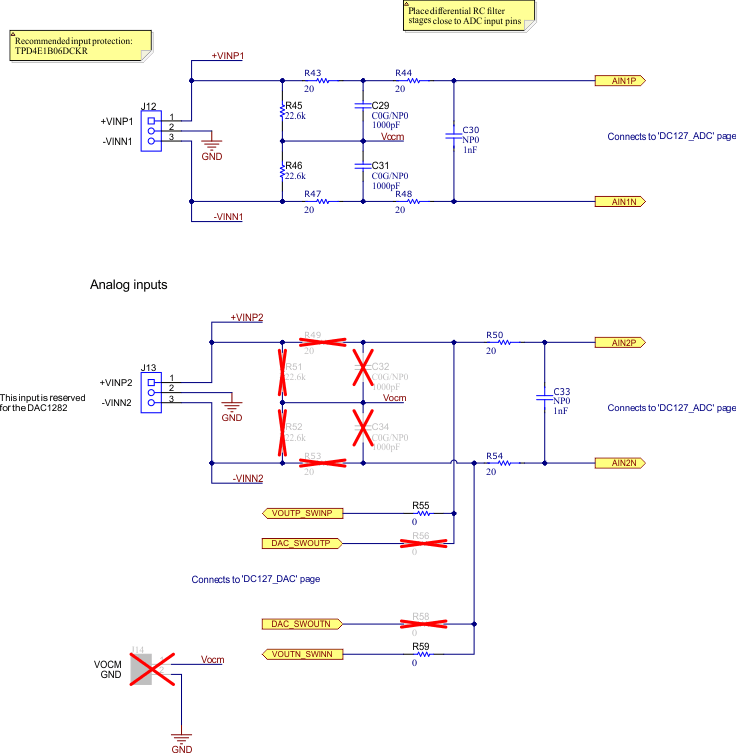
Analog inputs to the EVM can be connected to either terminal block associated with each ADC channel. The screw terminal blocks (J12, and J13) can interface directly with the leads of an external sensor input. Figure 3-1 depicts the signal chain used for the two input channels on the EVM and Table 3-1 lists the supported input options.
An input must not be applied such that the voltage on the input pins of the ADS1285 exceeds the absolute maximum ratings. For more details, see the ADS1285 data sheet.
R45 and R46 provide common-mode voltage paths for the channel 1 inputs. See Section 5 for more information. In addition, R43 and C29 (in combination with R47 and C31) provide the common-mode, low-pass filters for the positive and negative inputs, respectively. Furthermore, R44 and R40 in combination with C30 provides the differential low-pass filter used in antialiasing. The series impedance is kept relatively low to maintain adequate total harmonic distortion (THD) performance. Similar differential and common-mode, low-pass filter footprints are present on all inputs.
Specifically for channel 2, the default configuration is set up to use the DAC1282 on the input. As a result, the common-mode filters for this configuration are not populated, and R50, R54, and C33 are optimized for the output of the DAC. There are two options for connecting the DAC to the channel 2 of the ADS1285: using the direct output of the DAC1282 or the integrated switches of the DAC1282. By default, the direct output of the DAC1282 is used by populating R55 and R59. As a result, using the integrated switches is achieved by depopulating R55 and R59, populating R56 and R58, and configuring the DAC using the GUI as described in Section 6. For best THD performance (approximately a 1-dB difference), use the direct output. For maximum flexibility, use the integrated switches.
 Figure 3-1 Input Terminal
Blocks and Headers (Schematic)
Figure 3-1 Input Terminal
Blocks and Headers (Schematic)| Terminal Block | Pin | Function | ADS1285 Input Pin(s) |
|---|---|---|---|
| J12 | 1 | Channel 1 positive input | +VINP1 (Eventually leading to AIN1P) |
| 2 | GND | AGND and DGND | |
| 3 | Channel 1 negative input | –VINN1 (Eventually leading to AIN1N) |
|
| J13 | 1 | Channel 2 positive input | +VINP2 (Eventually leading to AIN2P) |
| 2 | GND | AGND and DGND | |
| 3 | Channel 2 negative input | –VINN2 (Eventually leading to AIN2N) |