SBOA242A January 2019 – October 2024 INA828 , OPA188 , TLV171
Design Goals
| Input | Output | Supply | |||
|---|---|---|---|---|---|
| ViMin | ViMax | VoMin | VoMax | Vcc | Vee |
| –13V | 13V | –14.85V | 14.85 | 15 | –15 |
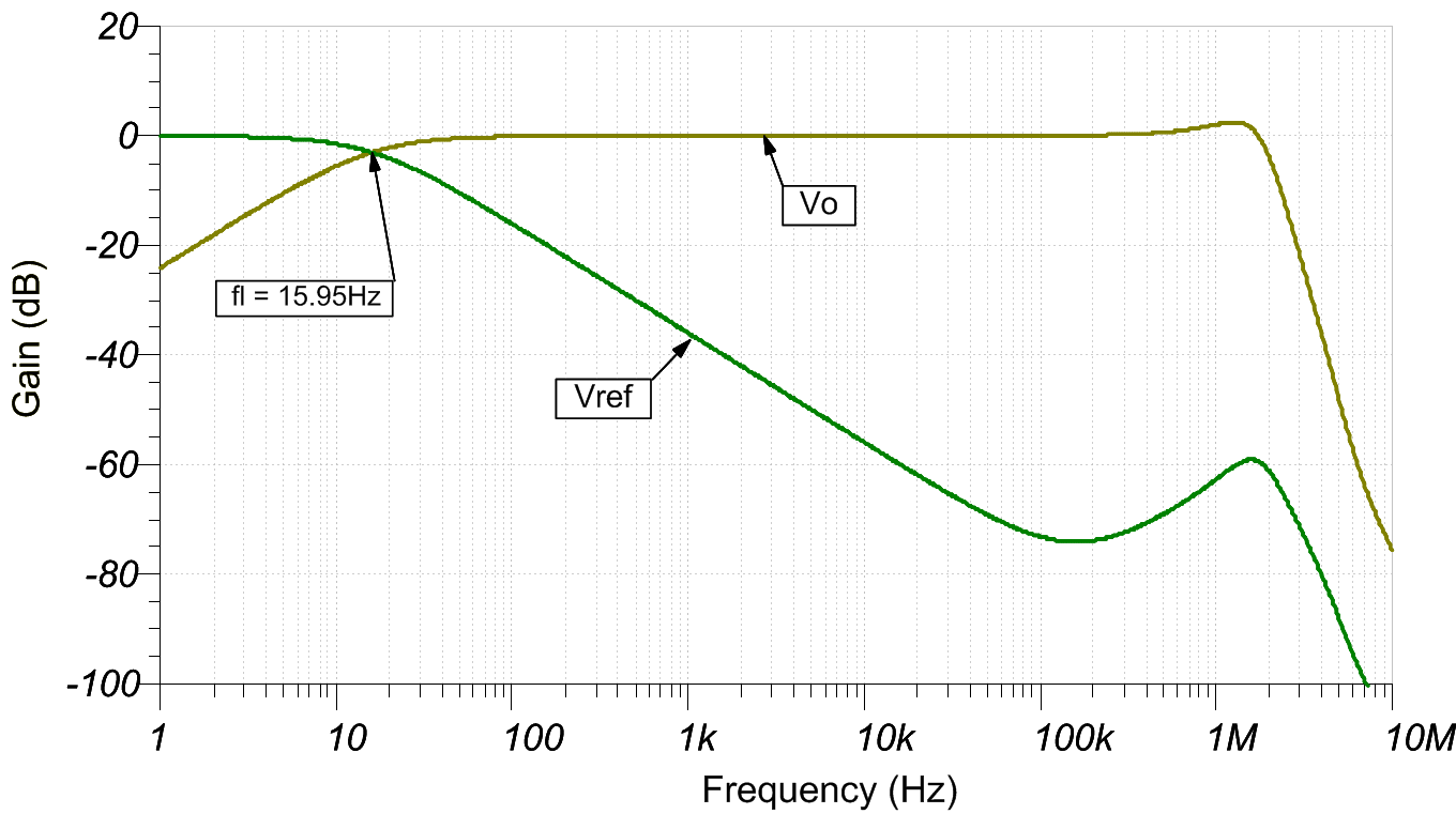
| Lower Cutoff Frequency (fL) | Gain | Input |
|---|---|---|
| 16Hz | 1 | ±2VAC; +10VDC |
Design Description
This circuit produces an AC-coupled output from a DC-coupled input to an instrumentation amplifier. The output is fed back through an integrator, and the output of the integrator is used to modulate the reference voltage of the amplifier. This creates a high-pass filter and effectively cancels the output offset. This circuit avoids the need for large capacitors and resistors on the input, which can significantly degrade CMRR due to component mismatch.
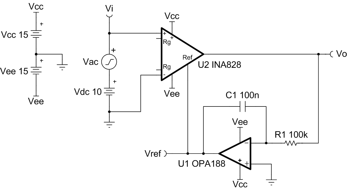
Design Notes
- The DC correction from output to reference is unity-gain. U1 can only correct for a signal within its input/output limitations, thus the magnitude of DC voltage that can be corrected for degrade with increasing instrumentation amplifier gain. See the table in Design Steps for more information.
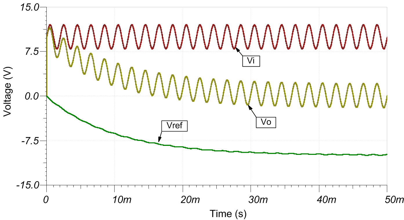
- Large values of R1 and C1 lower the cutoff frequency, but increase start up transient response time. Start up behavior is observed in the Transient Simulation Results.
- When AC-coupling this way, the total input voltage must remain within the common-mode input range of the instrumentation amplifier.
Design Steps
- Set the lower cutoff frequency for
circuit (integrator cutoff frequency). The upper cutoff frequency is dictated by
the gain and instrumentation amplifier bandwidth.
- Choose a standard value for
R1 and C1.
- The DC rejection capabilities of
the circuit degrade with gain. The following table provides a good estimate of
the DC correction range for higher gains.
Gain DC Correction Range 1V/V ±10V 10V/V ±1V 100V/V ±0.1V 1000V/V ±0.01V
Design Simulations
AC Simulation Results
Transient Simulation Results
Design References
Texas Instruments, SBOMAU0 TINA-TI™ circuit simulation, file download
Texas Instruments, TIPD191 Instrumentation Amplifier with DC Rejection, reference design
Design Featured Instrumentation Amplifier
| INA828 | |
|---|---|
| Vss | 4.5V to 36V |
| VinCM | Vee+2V to Vcc–2V |
| Vout | Vee+150mV to Vcc–150mV |
| Vos | 20µV |
| Iq | 600µA |
| Ib | 150pA |
| UGBW | 2MHz |
| SR | 1.2V/µs |
| #Channels | 1 |
| INA828 | |
Design Featured Op Amp
| OPA188 | |
|---|---|
| Vss | 8V to 36V |
| VinCM | Vee to Vcc–1.5V |
| Vout | Rail-to-rail |
| Vos | 6µV |
| Iq | 450µA |
| Ib | ±160pA |
| UGBW | 2MHz |
| SR | 0.8V/µs |
| #Channels | 1, 2, and 4 |
| OPA188 | |
Design Alternate Op Amp
| TLV171 | |
|---|---|
| Vss | 2.7V to 36V |
| VinCM | Vee–0.1V to Vcc–2V |
| Vout | Rail-to-rail |
| Vos | 750µV |
| Iq | 525µA |
| Ib | ±10pA |
| UGBW | 3MHz |
| SR | 1.5V/µs |
| #Channels | 1, 2, and 4 |
| TLV171 | |