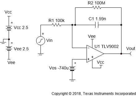
Integrator Circuit
Design Goals
| Input | Output | Supply | ||||
|---|---|---|---|---|---|---|
| fMin | f0dB | fMax | VoMin | VoMax | Vcc | Vee |
| 100 Hz | 1 kHz | 100 kHz | –2.45V | 2.45V | 2.5V | –2.5V |
Design Description
The integrator circuit outputs the integral of the input signal over a frequency range based on the circuit time constant and the bandwidth of the amplifier. The input signal is applied to the inverting input so the output is inverted relative to the polarity of the input signal. The ideal integrator circuit saturates to the supply rails depending on the polarity of the input offset voltage and requires the addition of a feedback resistor, R2, to provide a stable DC operating point. The feedback resistor limits the lower frequency range over which the integration function is performed. This circuit is most commonly used as part of a larger feedback/servo loop which provides the DC feedback path, thus removing the requirement for a feedback resistor.
Design Notes
- Use as large of a value as practical for the feedback resistor.
- Select a CMOS op amp to minimize the errors from the input bias current.
- The gain bandwidth product (GBP) of the amplifier will set the upper frequency range of the integrator function. The effectiveness of the integration function is usually reduced starting about one decade away from the amplifier bandwidth.
- An adjustable reference needs to be connected to the non-inverting input of the op amp to cancel the input offset voltage or the large DC noise gain will cause the circuit to saturate. Op amps with very low offset voltage may not require this.
Design Steps
The ideal circuit transfer function is given below.
- Set R1 to a standard
value.
- Calculate C1 to set the
unity-gain integration frequency.
- Calculate R2 to set the
lower cutoff frequency a decade less than the minimum operating frequency.
- Select an amplifier with a gain bandwidth at least 10 times the desired maximum operating frequency.
Design Simulations
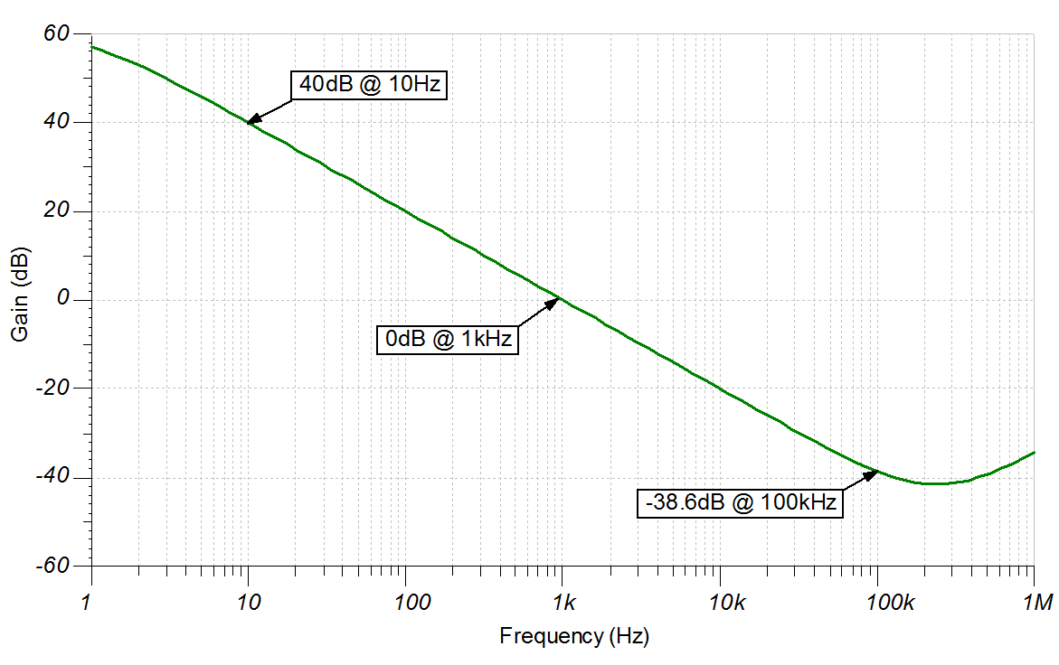
AC Simulation Results
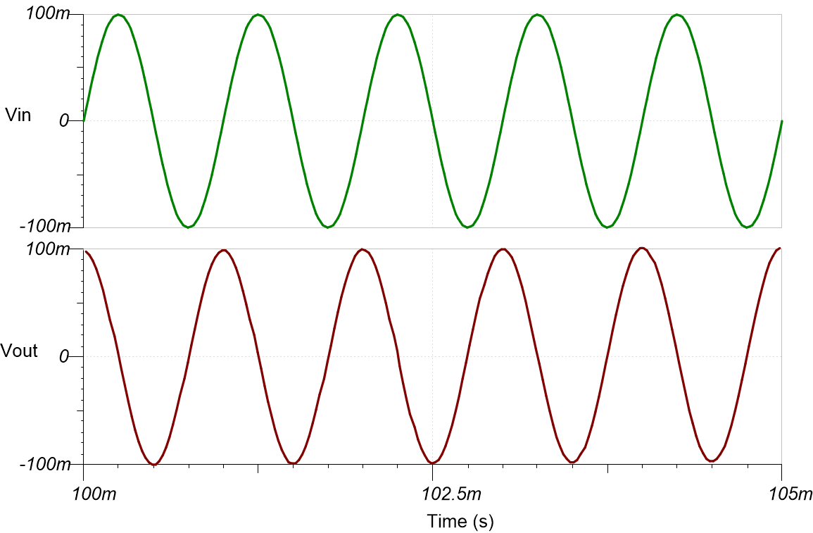
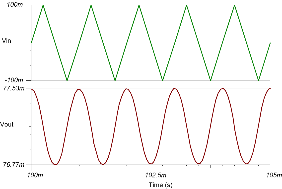
Transient Simulation Results
A 1kHz sine wave input yields a 1kHz cosine output.
A 1kHz triangle wave input yields a 1kHz sine wave output.
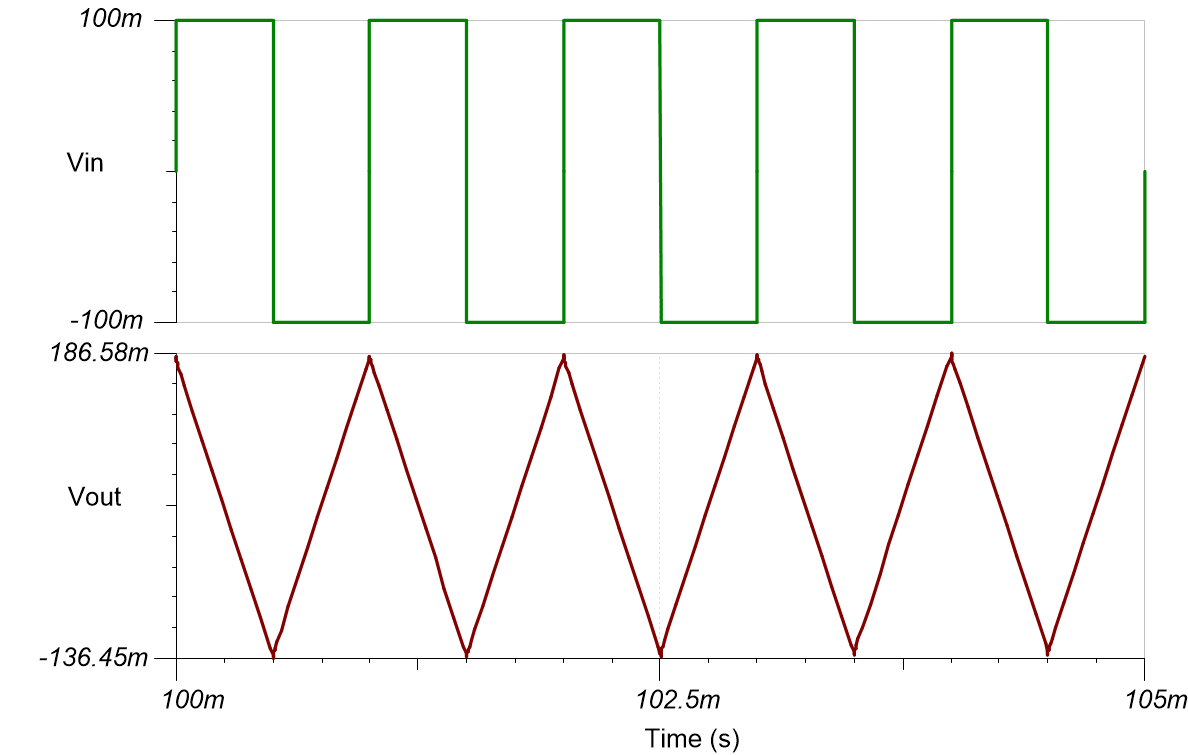
A 1kHz square wave input yields a 1kHz triangle wave output.
Design References
Texas Instruments, Simulation for Integrator Circuit, SBOC496 tool
Texas Instruments, Instrumentation Amplifier with DC Rejection, TIPD191 reference design
Design Featured Op Amp
| TLV9002 | |
|---|---|
| Vcc | 1.8V to 5.5V |
| VinCM | Rail-to-rail |
| Vout | Rail-to-rail |
| Vos | 0.4mV |
| Iq | 0.06mA |
| Ib | 5pA |
| UGBW | 1MHz |
| SR | 2V/µs |
| #Channels | 1, 2, and 4 |
| TLV9002 | |
Design Alternate Op Amp
| OPA376 | |
|---|---|
| Vcc | 2.2V to 5.5V |
| VinCM | (Vee-0.1V) to (Vcc-1.3V) |
| Vout | Rail-to-rail |
| Vos | 0.005mV |
| Iq | 0.76mA |
| Ib | 0.2pA |
| UGBW | 5.5MHz |
| SR | 2V/µs |
| #Channels | 1, 2, and 4 |
| OPA376 | |
