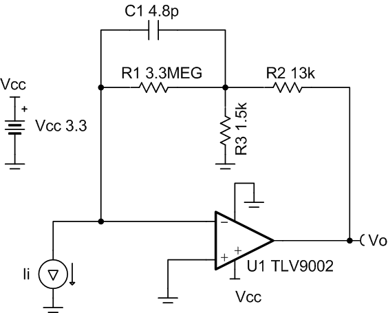
Transimpedance amplifier with T-network circuit
Design Goals
| Input | Output | BW | Supply | |||
|---|---|---|---|---|---|---|
| IiMin | IiMax | VoMin | VoMax | fp | Vcc | Vee |
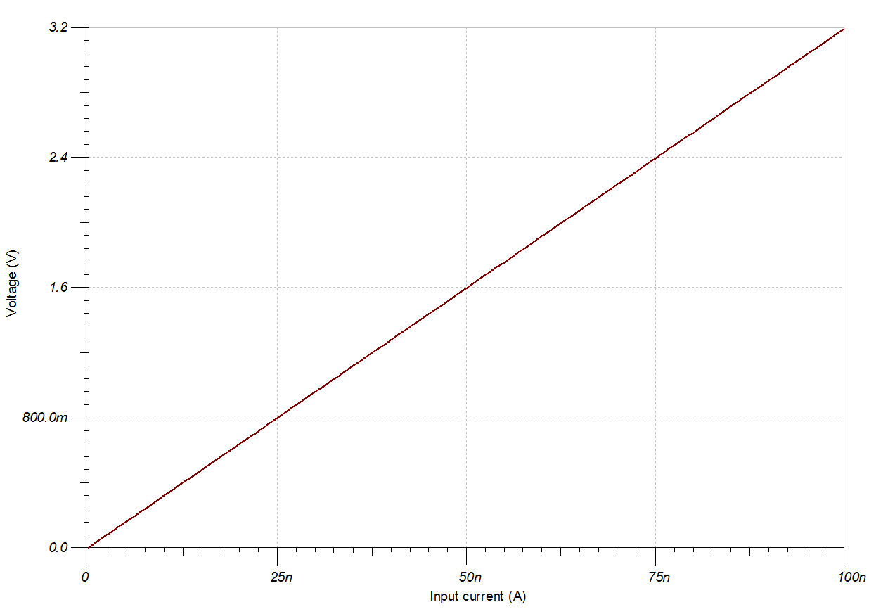
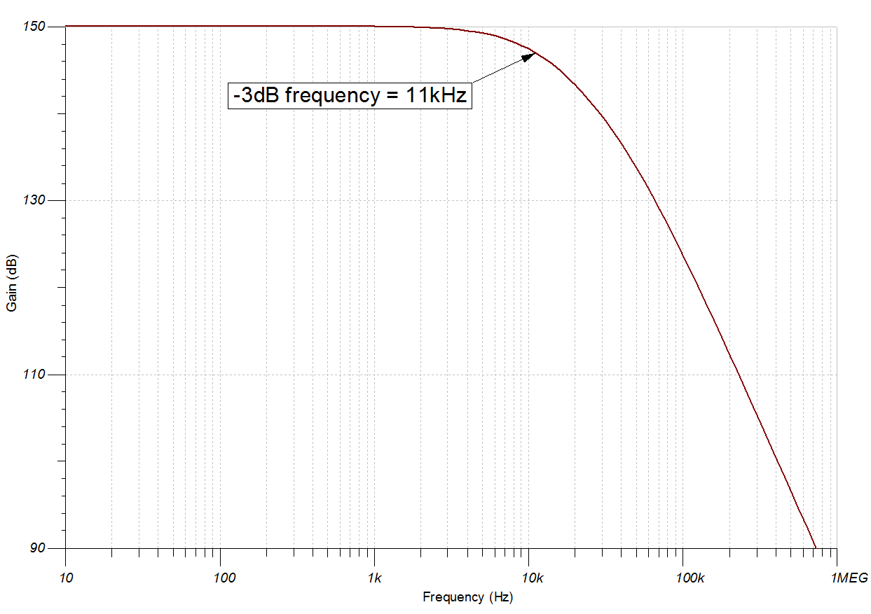
| 0A | 100nA | 0V | 3.2V | 10kHz | 3.3V | 0V |
Design Description
This transimpedance amplifier with a T-network feedback configuration converts an input current into an output voltage. The current-to-voltage gain is based on the T-network equivalent resistance which is larger than any of the resistors used in the circuit. Therefore, the T-network feedback configuration circuit allows for very high gain without the use of large resistors in the feedback or a second gain stage, reducing noise, stability issues, and errors in the system.
Design Notes
- C1 and R1 set the input signal cutoff frequency, fp.
- Capacitor C1 in parallel with R1 helps limit the bandwidth, reduce noise, and also improve the stability of the circuit if high-value resistors are used.
- The common-mode voltage is the voltage at the non-inverting input and does not vary with input current.
- A bias voltage can be added to the non-inverting input to bias the output voltage above the minimum output swing for 0A input current.
- Using high-value resistors can degrade the phase margin of the circuit and introduce additional noise in the circuit.
- Avoid placing capacitive loads directly on the output of the amplifier to minimize stability issues.
- For more information on op amp linear operating region, stability, slew-induced distortion, capacitive load drive, driving ADCs, and bandwidth see the Design References section.
Design Steps
The transfer function of this circuit follows:
- Calculate the required gain: Equation 1.
- Choose the resistor values to set the pass-band gain: Equation 1.
Since R1 will be the largest resistor value in the system choose this value first then choose R2 and calculate R3. Select R1 = 3.3MΩ and R2 = 13kΩ. R1 is very large due to the large transimpedance gain of the circuit. R2 is in the ~10k ohm range so the op amp can drive it easily.
Equation 1. - Calculate C1 to set the location of fp. Equation 1.
- Run a stability analysis to make sure that the circuit is stable. For more information on how to run a stability analysis see the TI Precision Labs - Op amp: Stability video.
Design Simulations
DC Simulation Results
AC Simulation Results
Design References
- See Analog Engineer's Circuit Cookbooks for TI's comprehensive circuit library.
- See SPICE file, SBOMB39.
- See TIPD176, www.ti.com/tool/tipd176.
- For more information on many op amp topics including common-mode range, output swing, bandwidth, and how to drive an ADC please visit TI Precision Labs.
Design Featured Op Amp
| TLV9002 | |
|---|---|
| Vcc | 1.8V to 5.5V |
| VinCM | Rail-to-rail |
| Vout | Rail–to–rail |
| Vos | 0.4mV |
| Iq | 60µA |
| Ib | 5pA |
| UGBW | 1MHz |
| SR | 2V/µs |
| #Channels | 1, 2, 4 |
| www.ti.com/product/TLV9002 | |
Design Alternate Op Amp
| OPA375 | |
|---|---|
| Vcc | 2.25V to 5.5V |
| VinCM | Vee to (Vcc –1.2V) |
| Vout | Rail–to–rail |
| Vos | 0.15mV |
| Iq | 890µA |
| Ib | 10pA |
| UGBW | 10MHz |
| SR | 4.75V/µs |
| #Channels | 1 |
| www.ti.com/product/OPA375 | |
IMPORTANT NOTICE AND DISCLAIMER
| TI PROVIDES TECHNICAL AND RELIABILITY DATA (INCLUDING DATASHEETS), DESIGN RESOURCES (INCLUDING REFERENCE DESIGNS), APPLICATION OR OTHER DESIGN ADVICE, WEB TOOLS, SAFETY INFORMATION, AND OTHER RESOURCES “AS IS” AND WITH ALL FAULTS, AND DISCLAIMS ALL WARRANTIES, EXPRESS AND IMPLIED, INCLUDING WITHOUT LIMITATION ANY IMPLIED WARRANTIES OF MERCHANTABILITY, FITNESS FOR A PARTICULAR PURPOSE OR NON-INFRINGEMENT OF THIRD PARTY INTELLECTUAL PROPERTY RIGHTS. |
| These resources are intended for skilled developers designing with TI products. You are solely responsible for (1) selecting the appropriate TI products for your application, (2) designing, validating and testing your application, and (3) ensuring your application meets applicable standards, and any other safety, security, or other requirements. These resources are subject to change without notice. TI grants you permission to use these resources only for development of an application that uses the TI products described in the resource. Other reproduction and display of these resources is prohibited. No license is granted to any other TI intellectual property right or to any third party intellectual property right. TI disclaims responsibility for, and you will fully indemnify TI and its representatives against, any claims, damages, costs, losses, and liabilities arising out of your use of these resources. |
| TI’s products are provided subject to TI’s Terms of Sale (www.ti.com/legal/termsofsale.html) or other applicable terms available either on ti.com or provided in conjunction with such TI products. TI’s provision of these resources does not expand or otherwise alter TI’s applicable warranties or warranty disclaimers for TI products. |
| Mailing Address: Texas Instruments, Post Office Box 655303, Dallas, Texas 75265
Copyright © 2020, Texas Instruments Incorporated |