SBOA285A December 2018 – September 2024 LPV821 , OPA375 , TLV9061
Design Goals
| Input | Output | Supply | Full–Scale Range Error | |||
|---|---|---|---|---|---|---|
| IiMax | ViMax | VoMin | VoMax | Vcc | Vee | FSRError |
| 1A | 250mV | 50mV | 4.9V | 5V | 0V | 0.2% |
Design Description
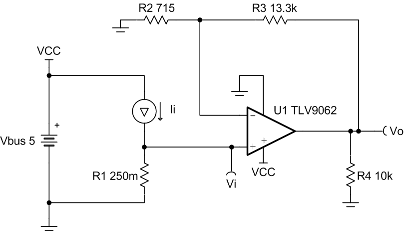
This single–supply, low–side, current sensing method accurately detects load current up to 1A and converts it to a voltage between 50mV and 4.9V. The input current range and output voltage range can be scaled as necessary and larger supplies can be used to accommodate larger swings.

Design Notes
- Use the op amp linear output operating range, which is usually specified under the test conditions.
- The common–mode voltage is equal to the input voltage.
- Tolerance of the shunt resistor and feedback resistors determines the gain error of the circuit.
- Avoid placing capacitive loads directly on the output of the amplifier to minimize stability issues.
- If trying to detect zero current with output swing to GND, a negative charge pump (such as LM7705) can be used as the negative supply in this design to maintain linearity for output signals near 0V. See Single-Supply, Low-Side, Unidirectional Current-Sensing Solution With Output Swing to GND Circuit analog engineer's circuit for more information.
- Using high–value resistors can degrade the phase margin of the circuit and introduce additional noise in the circuit.
- The small–signal bandwidth of this circuit depends on the gain of the circuit and gain bandwidth product (GBP) of the amplifier.
- Filtering can be accomplished by adding a capacitor in parallel with R3 . Adding a capacitor in parallel with R3 improves stability of the circuit if high–value resistors are used.
- For more information on op amp linear operating region, stability, capacitive load drive, driving ADCs, and bandwidth please see the Design References section.
Design Steps
The transfer function for this circuit is given below.
- Define the full–scale shunt voltage and calculate the
maximum shunt resistance.
- Calculate the gain required for maximum linear
output voltage.
- Select standard values for R2 and
R3.
From Analog Engineer’s calculator, use “Find Amplifier Gain” and get resistor values by inputting gain ratio of 19.6.
R2 = 715 Ω (0.1% Standard Value)
R3 = 13.3 kΩ (0.1% Standard Value)
- Calculate minimum
input current before hitting output swing–to–rail limit.
IiMin represents the minimum accurately
detectable input current.
- Calculate Full
scale range error and relative error. Vos is the
typical offset voltage found in data sheet.
- To maintain
sufficient phase margin, verify that the zero created by the gain setting resistors and
input capacitance of the device is greater than the bandwidth of the circuit
Design Simulations
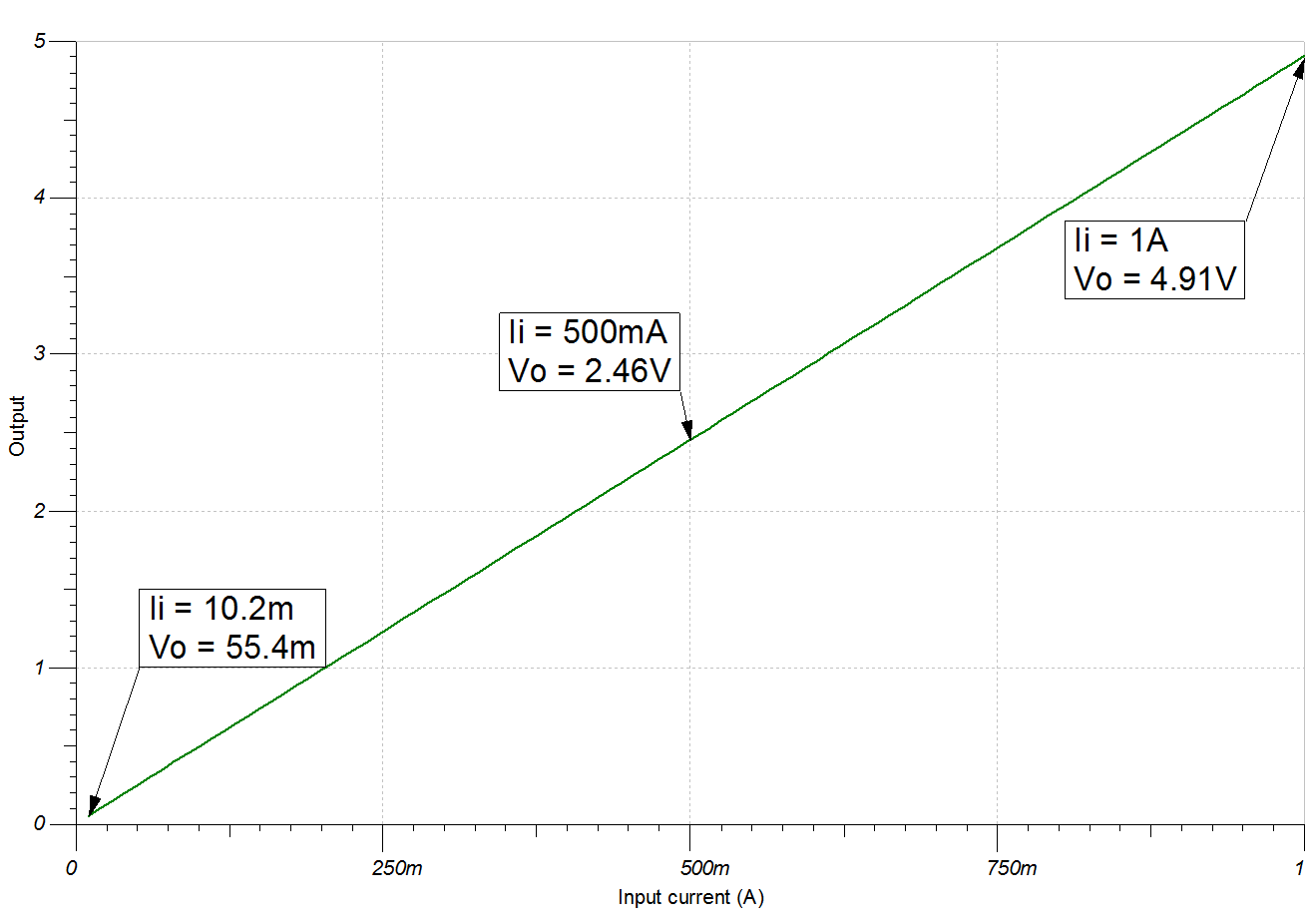
DC Simulation Results

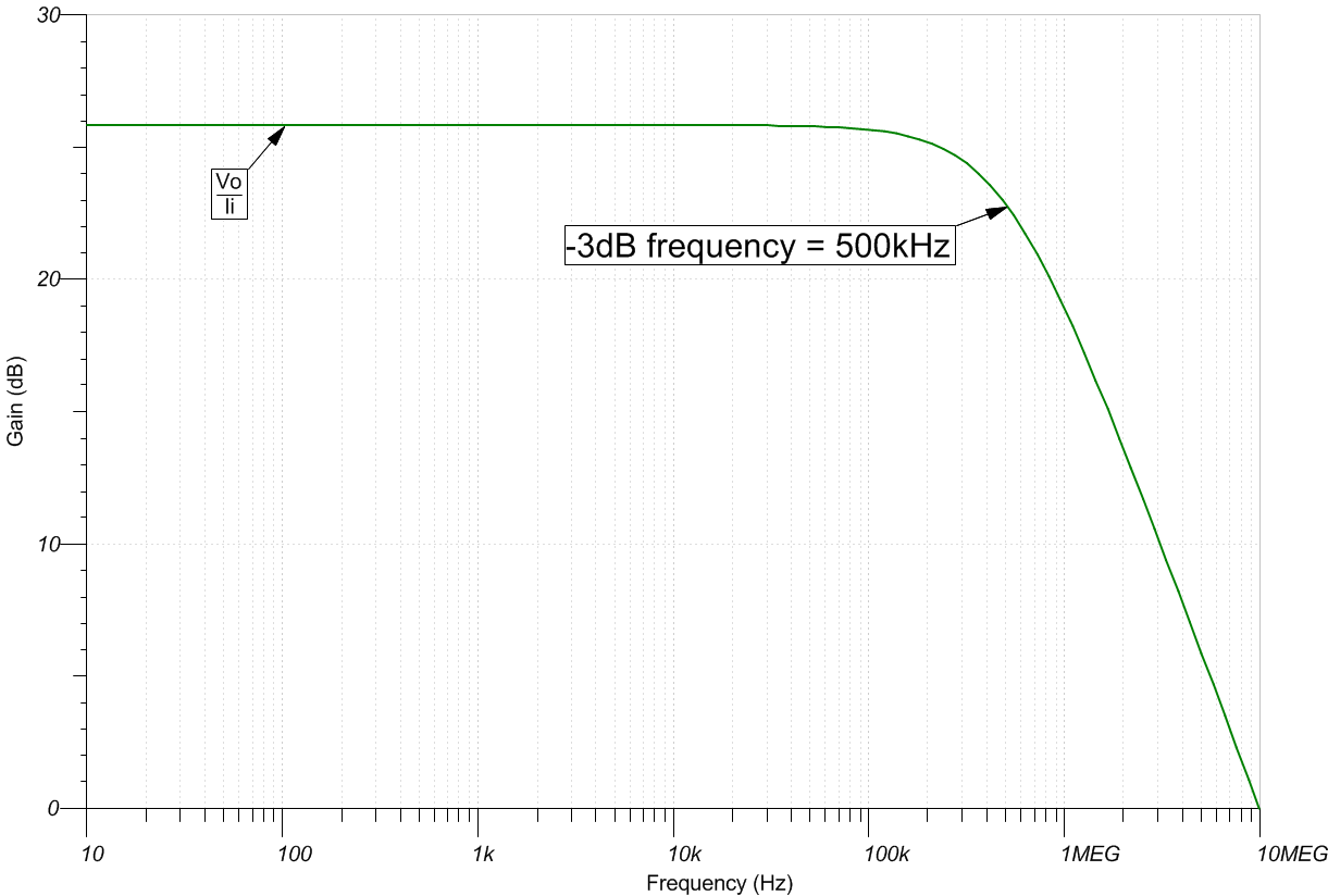
AC Simulation Results

References
Texas Instruments, Simulation for Single-Supply Low-Side Unidirectional Current-Sense Circuit, SBOC523 SPICE simulation file
Texas Instruments, 0-1A, Single-Supply, Low-Side, Current Sensing Solution, TIPD129 reference design
Texas Instruments, Current sensing reference design for 10µA to 10mA, low side, single supply, TIPD104 reference design
Texas Instruments, Single-Supply, Low-Side, Unidirectional Current-Sensing Solution With Output Swing to GND Circuit, analog engineer's circuit
Design Featured Op Amp
| TLV9061 | |
|---|---|
| Vss | 1.8V to 5.5V |
| VinCM | Rail–to–rail |
| Vout | Rail–to–rail |
| Vos | 0.3mV |
| Iq | 538µA |
| Ib | 0.5pA |
| UGBW | 10MHz |
| SR | 6.5V/µs |
| #Channels | 1,2,4 |
| TLV9061 | |
Design Alternate Op Amp
| OPA375 | |
|---|---|
| Vcc | 2.25V to 5.5V |
| VinCM | (V–) to ((V+)–1.2V) |
| Vout | Rail–to–rail |
| Vos | 0.15mV |
| Iq | 890µA |
| Ib | 10pA |
| UGBW | 10MHz |
| SR | 4.75V/µs |
| #Channels | 1 |
| OPA375 | |
For battery operated or power conscious designs, outside of the original design goals described earlier, where lowering total system power is desired.
| LPV821 | |
|---|---|
| Vcc | 1.7V to 3.6V |
| VinCM | Rail–to–rail |
| Vout | Rail–to–rail |
| Vos | 1.5µV |
| Iq | 650nA/Ch |
| Ib | 7pA |
| UGBW | 8kHz |
| SR | 3.3V/ms |
| #Channels | 1 |
| LPV821 | |