SBOA290A December 2018 – September 2024 TLV6741
Design Goals
| Input Pressure (Max) | Output Voltage (Max) | Supply | Frequency Response Deviation | ||
|---|---|---|---|---|---|
| 100dB SPL (2Pa) | 1.228Vrms | Vcc | Vee | 20Hz | 20kHz |
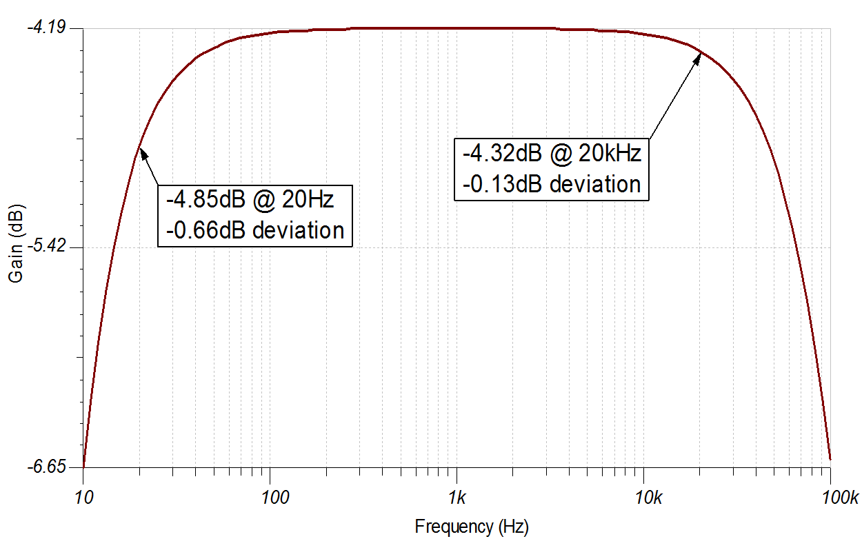
| 5V | 0V | –0.5dB | –0.1dB | ||
Design Description
This circuit uses a non–inverting amplifier circuit configuration to amplify the microphone output signal. This circuit has very good magnitude flatness and exhibits minor frequency response deviations over the audio frequency range. The circuit is designed to be operated from a single 5V supply.
Design Notes
- Operate within the op amp linear output operating range, which is usually specified under the AOL test conditions.
- Use low–K capacitors (tantalum, C0G, and so forth) and thin film resistors help to decrease distortion.
- Use a battery to power this circuit to eliminate distortion caused by switching power supplies.
- Use low value resistors and low noise op amps for low noise designs.
- The common mode voltage is equal to the DC bias voltage set using the resistor divider plus any variation caused by the microphone output voltage. For op amps with a complementary pair input stage it is recommended to keep the common mode voltage away from the cross over region to eliminate the possibility of cross over distortion.
- Resistor R1 is used to bias the microphone internal JFET transistor to achieve the bias current specified by the microphone.
- The equivalent input resistance is determined by R1, R2, R3. Use large value resistors for R2 and R3 to increase the input resistance.
- The voltage connected to R1 to bias the microphone does not have to be the same as the op amp supply voltage. Using a higher voltage supply for the microphone bias allows for a lower bias resistor value.
Design Steps
This design procedure uses the microphone specifications provided in the following table.
| Microphone Parameter | Value |
|---|---|
| Sensitivity at 94dB SPL (1Pa) | –35 ± 4dBV |
| Current Consumption (Max) | 0.5mA |
| Impedance | 2.2kΩ |
| Standard Operating Voltage | 2Vdc |
- Convert the sensitivity to volts per Pascal.
- Convert volts per Pascal to current per Pascal.
- Max output current occurs at max pressure 2Pa.
- Calculate bias resistor. In the
following equation, Vmic is microphone standard operating voltage.
- Set the amplifier input common mode
voltage to mid–supply voltage. The equivalent resistance of R2 in
parallel with R3 is 10 times larger than R1 so that a majority of the
microphone current flows through R1.
- Calculate the maximum input
voltage.
- Calculate gain required to produce
the largest output voltage swing.
- Calculate R4 to set the
gain calculated in 7. Select feedback resistor R5 as 10kΩ.
- Calculate the corner frequency at
low frequency according to the allowed deviation at 20Hz. In the following
equation, G_pole1 is the gain contributed by each pole at frequency "f." Note
that you divide by three because there are three poles.
- Calculate C1 based on
the cut off frequency calculated in 9.
- Calculate C2 based on
the cut off frequency calculated in 9.
- Calculate the high frequency pole
according to the allowed deviation at 20kHz. In the following equation, G_pole2
is the gain contributed by each pole at frequency "f."
- Calculate C3 to set the cut off
frequency calculated in 12.
- Calculate the output capacitor,
C4, based on the cut off frequency calculated in 9. Assume the output load R6 is 10kΩ.
Design Simulations
AC Simulation Results
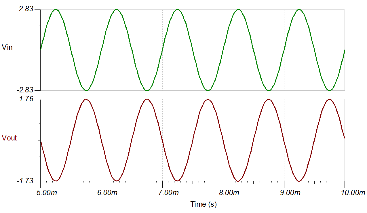
Transient Simulation Results
The input voltage represents the SPL of an input signal to the microphone. A 1Vrms input signal represents 1Pa.
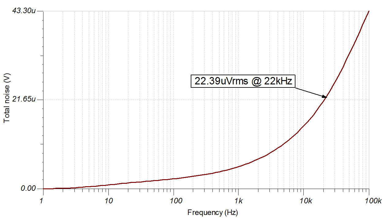
Noise Simulation Results
The following simulation results show 22.39uVrms of noise at 22kHz. The noise is measured at a bandwidth of 22kHz to represent the measured noise using an audio analyzer with the bandwidth set to 22kHz.
References:
Texas Instruments, Simulation for Non-Inverting Microphone Amplifier Circuit, SBOC525 SPICE simulation file
TI Precision Designs Single-Supply, Electret Microphone Preamplifier, TIPD181 reference design
Design Featured Op Amp
| TLV6741 | |
|---|---|
| Vss | 1.8V to 5.5V |
| VinCM | (Vee) to (Vcc –1.2V) |
| Vout | Rail–to–rail |
| Vos | 150µV |
| Iq | 890uA/Ch |
| Ib | 10pA |
| UGBW | 10MHz |
| SR | 4.75V/µs |
| #Channels | 1 |
| TLV6741 | |
Design Alternate Op Amp
| OPA320 | |
|---|---|
| Vss | 1.8V to 5.5V |
| VinCM | Rail–to–rail |
| Vout | Rail–to–rail |
| Vos | 40µV |
| Iq | 1.5mA/Ch |
| Ib | 0.2pA |
| UGBW | 20MHz |
| SR | 10V/µs |
| #Channels | 1, 2 |
| OPA320 | |