SBOA306C September 2018 – July 2024 TLV1832 , TLV1842
Design Goals
| Load Current (IL) | System Supply (VS) | Comparator Output Status | ||
|---|---|---|---|---|
| Overcurrent (IOC) | Recovery Current (IRC) | Typical | Overcurrent | Normal Operation |
| 1A | 0.5A | 10V | VOL < 0.4V | VOH = VPU = 3.3V |
Design Description
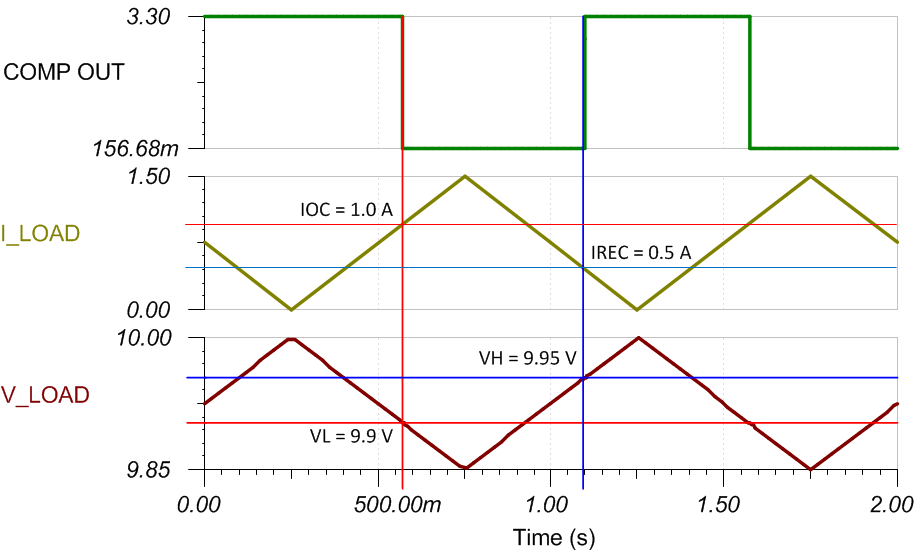
This high-side, current sensing circuit uses one comparator with a rail-to-rail input common-mode range to create an overcurrent alert (OC-Alert) signal at the comparator output (COMP OUT) if the load current rises above 1A. The OC-Alert signal in this implementation is active low. So when the 1A threshold is exceeded, the comparator output goes low. Hysteresis is implemented such that OC-Alert returns to a logic high state when the load current reduces to 0.5A (a 50% reduction). This circuit utilizes an open-drain output comparator to level shift the output high logic level for controlling a digital logic input pin. For applications needing to drive the gate of a MOSFET switch, a comparator with a push-pull output is preferred.

Design Notes
- Select a comparator with rail-to-rail input common-mode range to enable high-side current sensing.
- Select a comparator with an open-drain output stage for level-shifting.
- Select a comparator with low input offset voltage to optimize accuracy.
- Calculate the value for the shunt resistor (R6) so the shunt voltage (VSHUNT) is at least ten times larger than the comparator offset voltage (VIO).
Design Steps
- Select the value of R6
so VSHUNT is at least 10 times greater than the comparator input
offset voltage (VIO). Making R6 very large improves OC
detection accuracy but reduces supply headroom.
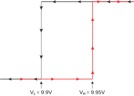
- Determine the desired switching
thresholds for when the comparator output transitions from high-to-low
(VL) and low-to-high (VH). VL represents
the threshold when the load current crosses the OC level, while VH
represents the threshold when the load current recovers to a normal operating
level.
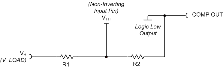
- With the non-inverting input pin of
the comparator labeled as VTH and the comparator output in a logic
low state (ground), derive an equation for VTH where VH
represents the load voltage (VLOAD) when the comparator output
transitions from low to high. Note that the simplified diagram for deriving the
equation shows the comparator output as ground (logic low).
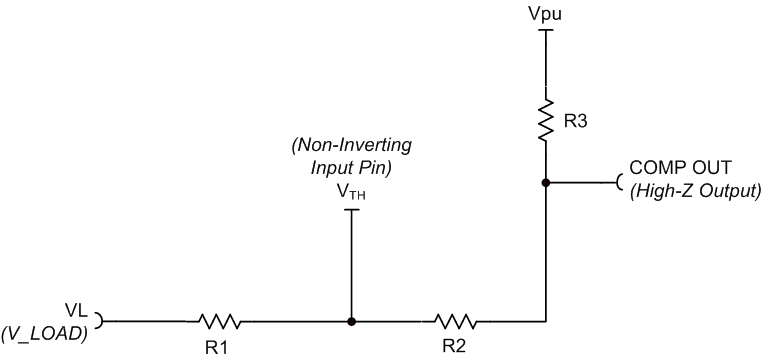
- With the non-inverting input pin of
the comparator labeled as VTH and the comparator output in a
high-impedance state, derive an equation for VTH where VL
represents the load voltage (VLOAD) when the comparator output
transitions from high to low. Applying superposition theory to solve for
VTH is recommended.
- Eliminate variable VTH
by setting the two equations equal to each other and solve for R1.
The result is the following quadratic equation. Solving for R2 is
less desirable since there are more standard values for small resistor values
than the larger ones.
- Select values for R3 and R2.
R3 is significantly smaller than R2 (R3
<< R2). Avoid increasing R3 since an increase in
R3 causes the comparator logic high-output level to increase
beyond VPU. For example, increasing R3 to a value of 100kΩ
can cause the logic high output to be 3.6V. In this case, select R2 =
2M and R3 = 1kΩ.
- Calculate R1 after
substituting in numeric values for VPU, R2, VL,
VH, and R3. For this design, set VPU = 3.3,
R2 = 2M, VL = 9.9, VH = 9.95, and
R3 = 1kΩ.
- Calculate VTH using the
equation derived in Design Step 3; use the calculated value for
R1. Note that VTH is less than VL since
VPU is less that VL.
- With the inverting terminal labeled
as VTH, derive an equation for VTH in terms of
R4, R5, and VS.
- Calculate R4 after
substituting in numeric values R5 = 1M, VS = 10, and the
calculated value for VTH.
Design Simulations
DC Simulation Results
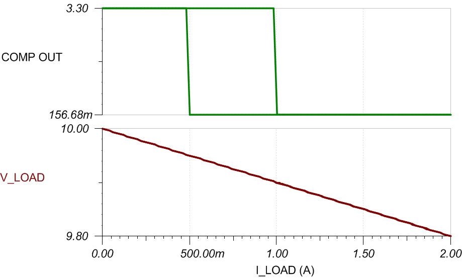
Transient Simulation Results
Design References
See Analog Engineer's Circuit Cookbooks for TI's comprehensive circuit library.
See Circuit SPICE Simulation File SLOM456.
Design Featured Comparator
| Parameters | TLV184x | TLV183x |
|---|---|---|
| VS | 2.7V to 40V | 2.7V to 40V |
| VinCM | 2.7V to 40V | 2.7V to 40V |
| VOUT | Open-Drain | Push-Pull |
| VOS | 500µV | 500µV |
| IQ | 70µA/Ch | 70µA/Ch |
| tPD(HL) | 65ns | 65ns |
| #Channels | 1, 2, 4 | 1, 2, 4 |
| TLV184x | TLV183x |
Design Alternate Comparator
| TLV902x_3x | TLV323x | |
|---|---|---|
| VS | 1.6V to 5.5V | 2.7V to 5.5V |
| VinCM | Rail-to-rail | Rail-to-rail |
| VOUT | Open-Drain, Push-Pull | Push-Pull |
| VOS | 300µV | 500µV |
| IQ | 16µA/Ch | 200µA/Ch |
| tPD(HL) | 100ns | 20ns |
| #Channels | 1, 2, 4 | 1, 2 |
| TLV902x_3x | TLV3231 |