SBOA324 May 2021 OPA172 , OPA2991 , TLV9042
Design Goals
| Input Current | Ambient light current | Output voltage | Target Bandwidth | Supply | |||
|---|---|---|---|---|---|---|---|
| IiMin | IiMax | VoMin | VoMax | Vcc | Vee | ||
| –10µA | 10µA | 100µA | 0.5V | 4.5V | 300kHz | 5V | 0V |
Design Description
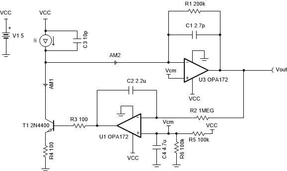
This circuit uses an op amp configured as a transimpedance amplifier to amplify the AC signal of a photodiode (modeled by Ii and C3). The circuit rejects DC signals using a transistor to sink DC current out of the photodiode through the use of an integrator in a servo loop. The bias voltage applied to the non-inverting input prevents the output from saturating to the negative supply rail in the absence of input current.
Design Notes
- Use a JFET or CMOS input op amp with low-bias current to reduce DC errors.
- A capacitor placed in parallel with the feedback resistor will limit bandwidth, improve stability and help reduce noise.
- The junction capacitance of photodiode changes with reverse bias voltage which will influence the stability of the circuit.
- Reverse-biasing the photodiode can reduce the effects of dark current.
- A resistor, R3, may be needed on the output of the integrator amplifier.
- An emitter degeneration resistor, R4, should be used to help stabilize the BJT.
- Use the op amp in a linear operating region. Linear output swing is usually specified under the AOL test conditions.
Design Steps
The transfer function of the circuit is:
- Calculate the value of the feedback resistor, R1, to produce the desired output swing.
- Calculate the feedback capacitor to limit the signal bandwidth.
- Calculate the gain bandwidth of the amplifier needed for the circuit to be stable.
Where:
Given:
- Cpd: Junction capacitance of photodiode
- Cb: Output capacitance of BJT
- Cd: Differential input capacitance of the amplifier
- Ccm: Common-mode input capacitance of the inverting input
- Set the cutoff frequency of the integrator circuit, fl, to 0.1Hz to only allow signals near DC to be subtracted from the photodiode output current. The cutoff frequency is set by R2 and C2. Select R2 as 1MΩ.
- Select R3 as 100Ω to isolate the capacitance of the BJT from op amp and stabilize the amplifier. For more information on stability analysis, see the Design References section [2].
- Bias the output of the circuit by setting the input common mode voltage of the integrator circuit to mid-supply. Select R5 and R6 as 100kΩ.
- Calculate capacitor C2 to filter the power supply and resistor noise. Set the cutoff frequency to 1Hz.
Design Simulations
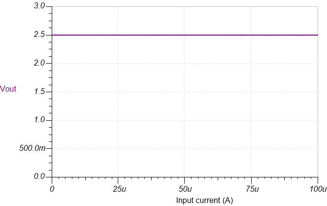
DC Simulation Results
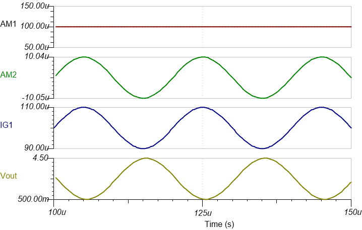
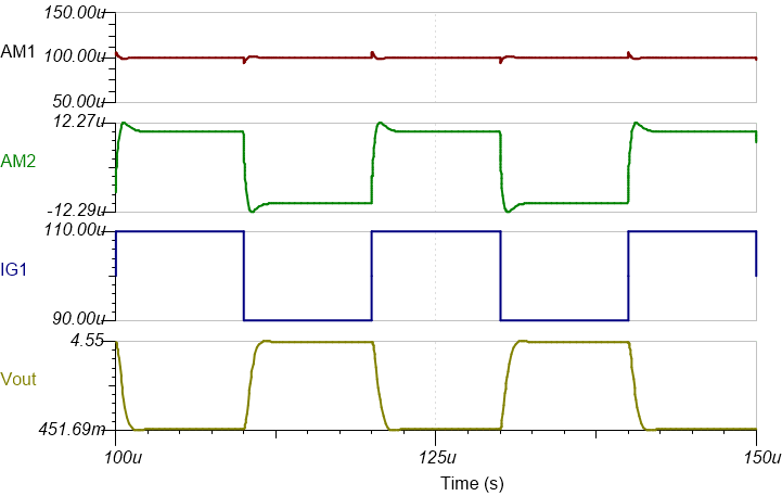
Transient Simulation Results
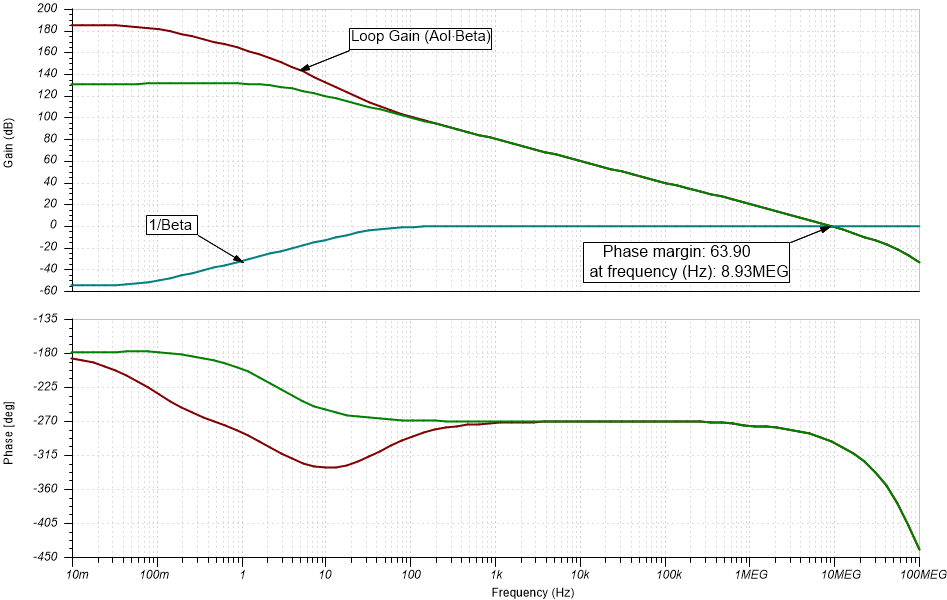
Integrator Open Loop Stability
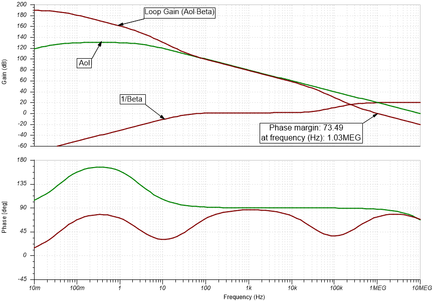
TIA Stability Results
Design References
- See Analog Engineer's Circuit Cookbooks for TI's comprehensive circuit library.
- TI Precision Labs
Design Featured Op Amp
| OPA172 | |
|---|---|
| Vcc | ±2.25V to ±18V, 4.5V to 36V |
| VinCM | (V–) – 0.1V to (V+) – 2V |
| Vout | Rail-to-rail |
| Vos | 0.2mV |
| Iq | 1.6mA |
| Ib | 8pA |
| UGBW | 10MHz |
| SR | 10V/µs |
| #Channels | 1,2,4 |
| www.ti.com/product/OPA172 | |
Design Alternate Op Amps
|
OPA2991 |
TLV9042 |
|
|---|---|---|
| Vss | ±1.35V to ±20V, 2.7V to 40V |
±0.6V to ±2.75V, 1.2V to 5.5V |
| VinCM | Rail-to-rail | Rail-to-rail |
| Vout | Rail-to-rail | Rail-to-rail |
| Vos | 125µV |
0.6mV |
| Iq | 560µV |
10uA |
| Ib | 1pA |
1pA |
| UGBW | 4.5MHz |
350kHz |
| SR | 20V/µs |
0.2V/us |
| #Channels | 1, 2, 4 |
1, 2, 4 |
| www.ti.com/product/OPA2991 | www.ti.com/product/TLV9042 |