SBOA331A January 2019 – September 2024 THS4131 , THS4561
Design Goals
| Input | Output | Supply | |
|---|---|---|---|
| Differential | Differential | Vcc | Vee |
| 1Vpp | 16Vpp | 10V | 0V |
| Output Common-Mode | 3dB Bandwidth | AC Gain (Gac) |
|---|---|---|
| 5V | 3MHz | 16V/V |
Design Description
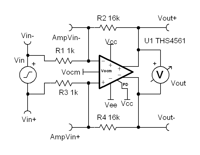
This design uses a fully differential amplifier (FDA) as a differential input to differential output amplifier.
Design Notes
- The ratio R2/R1, equal to R4/R3, sets the gain of the amplifier.
- For a given supply, the output swing for and FDA is twice that of a single ended amplifier. This is because a fully differential amplifier swings both terminals of the output, instead of swinging one and fixing the other to either ground or a Vref. The minimum voltage of an FDA is therefore achieved when Vout+ is held at the negative rail and Vout- is held at the positive rail, and the maximum is achieved when Vout+ is held at the positive rail and Vout- is held at the negative rail.
- FDAs are useful for noise sensitive signals, since noise coupling equally into both inputs will not be amplified, as is the case in a single ended signal referenced to ground.
- The output voltages will be centered about the output common-mode voltage set by Vocm.
- Both feedback paths should be kept symmetrical in layout.
Design Steps
- Set the ratio R2/ R1 to select the
AC voltage gain. To keep the feedback paths balanced,

- Given the output rails of 9.8 V and 0.2 V for Vs = 10 V, verify
that 16 Vpp falls within the output range available for Vocm = 5 V.
In normal operation:

- Rearrange to solve for each output voltage in edge conditions
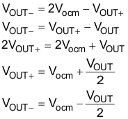
- Verifying for Vout = +8 V and
Vocm = +5 V,

- Verifying for Vout = -8 V and
Vocm = +5 V,

Note that the maximum swing possible is:

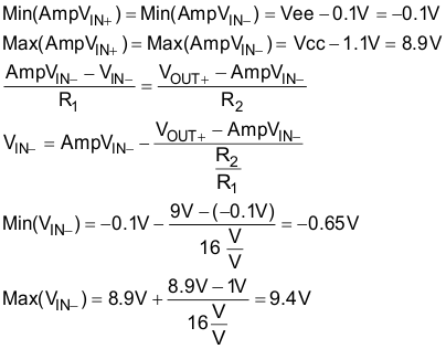
- Use the input common mode voltage range
of the amplifier and the feedback resistor divider to find the signal input
range when the output range is 1 V to 9 V. Due to symmetry, calculation of one
side is sufficient.
Design Simulations
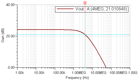 AC Simulation Results
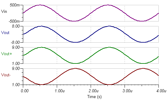 Transient Simulation Results
Design References
Texas Instruments, High-Q Active Differential Bandpass Filter Reference Design for Instrumentation Qualification, TIDA-01036 tool folder
Design Featured Op Amp
| THS4561 | |
|---|---|
| Vss | 3V to 13.5V |
| VinCM | Vee-0.1V to Vcc-1.1V |
| Vout | Vee+0.2V to Vcc-0.2 |
| Vos | TBD |
| Iq | TBD |
| Ib | TBD |
| UGBW | 70MHz |
| SR | 4.4V/µs |
| #Channels | 1 |
| THS4561 | |
Design Alternate Op Amp
| THS4131 | |
|---|---|
| Vss | 5V to 33V |
| VinCM | Vee+1.3V to Vcc-0.1V |
| Vout | Varies |
| Vos | 2mV |
| Iq | 14mA |
| Ib | 2µA |
| UGBW | 80MHz |
| SR | 52V/µs |
| #Channels | 1 |
| THS4131 | |