SBOA585 March 2024 ADS127L11 , ADS127L11 , ADS127L21 , ADS127L21 , PGA849 , PGA849 , PGA855 , PGA855
- 1
- Abstract
- Trademarks
- 1PGA855 and ADS127L21, 24-Bit, Delta-Sigma ADC Driver Circuit
- 2PGA855 Analog Front-End Filters
- 3ADS127Lx1 Delta-Sigma ADC and Digital Filter
- 4Approximate PGA855 Intrinsic Noise Analysis
- 5PGA855 and ADS127Lx1 System Noise
- 6PGA855 and ADS127Lx1 SNR and Noise Calculator
- 7PGA855 and ADS127Lx1 FFT Measured Performance
- 8Summary
- 9References
7 PGA855 and ADS127Lx1 FFT Measured Performance
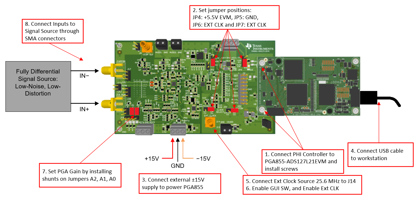
Figure 7-13 shows a block diagram for the PGA855-ADS127L21 circuit as tested on the bench.
A 1-kHz sine-wave test signal generates the SNR and THD data. The signal source must provide better noise performance and lower distortion than the circuit under test. The bench set up uses a low-pass filter between the signal source and PGA855 circuit to help reduce extrinsic noise injected into the circuit. The amplitude is adjusted to provide a –0.2-dBFS output from the ADC.
The bench set up uses an external low-jitter clock source of 25.6MHz as shown on Figure 7-13 to obtain a 200 kSPS data rate.
The PGA855 circuit is configured as shown in Figure 7-13. An equivalent resistance of 1kΩ is added in series between the signal source and PGA855 circuit, to account for the noise contribution of the 2kΩ bridge sensor resistance. The ADS127Lx1 GUI is configured with the ADC input buffers enabled and high-reference range selected.
 Figure 7-1 PGA855-ADS127L21 Bench
Test
Figure 7-1 PGA855-ADS127L21 Bench
TestTable 7-6 lists the ADC settings, reference voltage on the PGA855-ADS127L21 bench measurements.
| PARAMETER | VALUE |
|---|---|
| Input voltages (VPP, differential) | 20V, 16V, 8V, 4V, 2V, 1V, 0.5V, 0.25V |
| ADC reference voltage | 4.096 |
| Data rate | 200.0 kSPS, OSR = 64 |
| Test frequency | 1 kHz |
| THD (gain = 1) | < –120dB typical |
| SNR (gain = 1, wideband filter) | > 108dB typical |
| SNR (gain = 1, sinc4 filter) | > 110dB typical |
Table 7-2 shows the SNR measurement of the PGA855 driving the ADS127L21 delta-sigma ADC using a sinc4 or wideband filter at 200kSPS. At gain = 1, the design achieves a 108.1-dB SNR for the wideband filter and 110.1-dB SNR for the sinc4 filter.
| PGA GAIN (V/V) | INPUT (VPEAK) | WIDEBAND SNR (dB) | SINC4 SNR (dB) | ||
|---|---|---|---|---|---|
| Calculated | Measured | Calculated | Measured | ||
| 0.125 | 20 | 108.5 | 106.0(1) | 110.5 | 107.6(1) |
| 0.25 | 16 | 108.4 | 108.4 | 110.4 | 110.4 |
| 0.5 | 8 | 108.4 | 108.4 | 110.4 | 110.4 |
| 1 | 4 | 108.3 | 108.1 | 110.3 | 110.1 |
| 2 | 2 | 107.5 | 107.2 | 109.6 | 109.3 |
| 4 | 1 | 105.5 | 105.0 | 107.9 | 107.1 |
| 8 | 0.5 | 101.2 | 100.6 | 103.8 | 103.0 |
| 16 | 0.25 | 95.7 | 95.0 | 98.5 | 97.2 |
Figure 7-7 and Figure 7-8 show the respective 1-kHz, full-scale FFT plots for the wideband and sinc4 filters at gain = 1. Because of the frequency roll-off of the sinc4 filter, SNR performance improves by an average of 2dB compared to the wideband filter. The filters provide identical THD results at –120-dB typical.

| G = 1V/V, fIN = 1kHz |

| G = 1V/V, fIN = 1kHz |