SBOS473L March   2009  – July 2024 TMP112 , TMP112D

PRODUCTION DATA  

  1.   1
  2. Features
  3. Applications
  4. Description
  5. Device Comparison
  6. Pin Configuration and Functions
  7. Specifications
    1. 6.1 Absolute Maximum Ratings
    2. 6.2 ESD Ratings
    3. 6.3 Recommended Operating Conditions
    4. 6.4 Thermal Information
    5. 6.5 Electrical Characteristics
    6. 6.6 Timing Requirements
    7. 6.7 Timing Diagrams
    8. 6.8 Typical Characteristics (TMP112A/B/N)
    9. 6.9 Typical Characteristics (TMP112Dx)
  8. Detailed Description
    1. 7.1 Overview
    2. 7.2 Functional Block Diagrams
    3. 7.3 Feature Description
      1. 7.3.1 Digital Temperature Output
      2. 7.3.2 Serial Interface
        1. 7.3.2.1 Bus Overview
        2. 7.3.2.2 Serial Bus Address
        3. 7.3.2.3 Writing and Reading Operation
        4. 7.3.2.4 Target Mode Operations
          1. 7.3.2.4.1 Target Receiver Mode
          2. 7.3.2.4.2 Target Transmitter Mode
        5. 7.3.2.5 SMBus Alert Function
        6. 7.3.2.6 General Call
        7. 7.3.2.7 High-Speed (Hs) Mode
        8. 7.3.2.8 Timeout Function
        9. 7.3.2.9 Timing Diagrams
          1. 7.3.2.9.1 Two-Wire Timing Diagrams
    4. 7.4 Device Functional Modes
      1. 7.4.1 Continuous-Conversion Mode
      2. 7.4.2 Extended Mode (EM)
      3. 7.4.3 One-Shot/Conversion Ready Mode (OS)
      4. 7.4.4 Thermostat Mode (TM)
        1. 7.4.4.1 Comparator Mode (TM = 0)
        2. 7.4.4.2 Interrupt Mode (TM = 1)
    5. 7.5 Programming
      1. 7.5.1 Pointer Register
      2. 7.5.2 Temperature Register
      3. 7.5.3 Configuration Register
        1. 7.5.3.1 Shutdown Mode (SD)
        2. 7.5.3.2 Thermostat Mode (TM)
        3. 7.5.3.3 Polarity (POL)
        4. 7.5.3.4 Fault Queue (F1/F0)
        5. 7.5.3.5 Converter Resolution (R1 and R0)
        6. 7.5.3.6 One-Shot (OS)
        7. 7.5.3.7 Extended Mode (EM)
        8. 7.5.3.8 Alert (AL)
      4. 7.5.4 High- and Low-Limit Register
  9. Application and Implementation
    1. 8.1 Application Information
    2. 8.2 Typical Application
      1. 8.2.1 Design Requirements
      2. 8.2.2 Detailed Design Procedure
      3. 8.2.3 Application Curve
      4. 8.2.4 Power Supply Recommendations
    3. 8.3 Layout
      1. 8.3.1 Layout Guidelines
      2. 8.3.2 Layout Example
  10. Device and Documentation Support
    1. 9.1 Documentation Support
      1. 9.1.1 Related Documentation
    2. 9.2 Receiving Notification of Documentation Updates
    3. 9.3 Support Resources
    4. 9.4 Trademarks
    5. 9.5 Electrostatic Discharge Caution
    6. 9.6 Glossary
  11. 10Revision History
  12. 11Mechanical, Packaging, and Orderable Information
    1. 11.1 Tape and Reel Information

Mechanical, Packaging, and Orderable Information

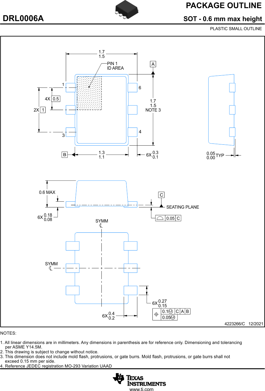
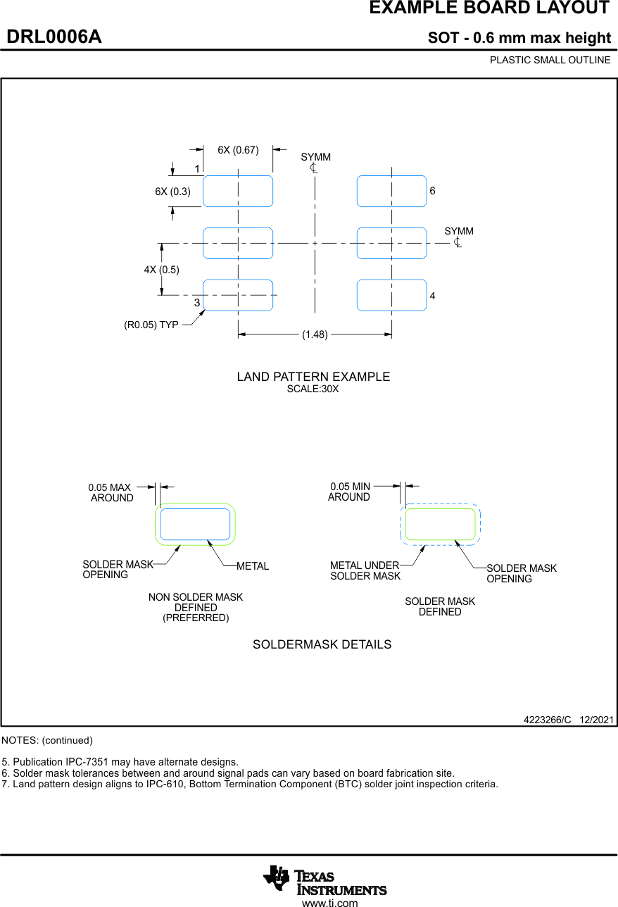
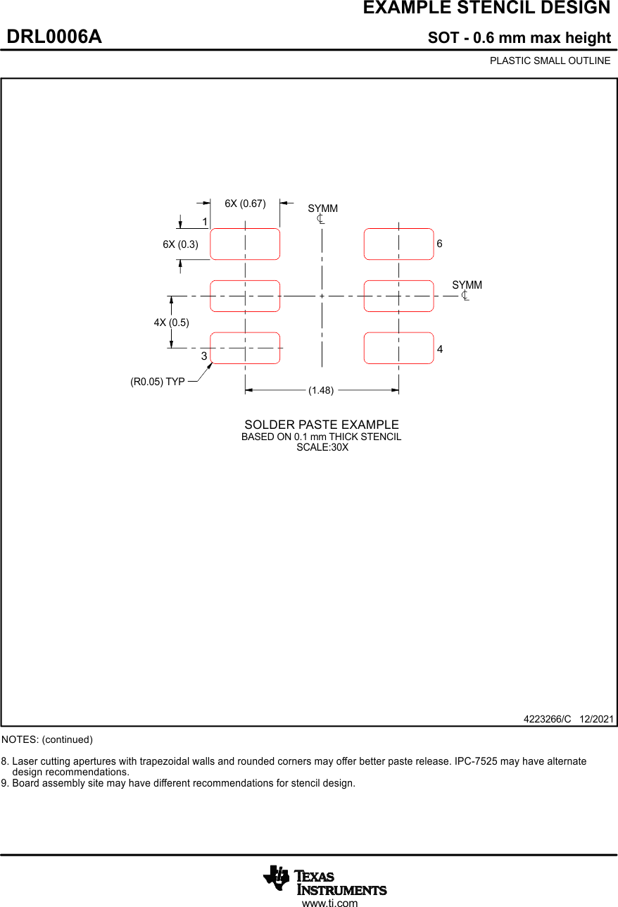
The following pages include mechanical, packaging, and orderable information. This information is the most current data available for the designated devices. This data is subject to change without notice and revision of this document. For browser-based versions of this data sheet, refer to the left-hand navigation.

TMP112 TMP112D
TMP112 TMP112D
TMP112 TMP112D
TMP112 TMP112D
TMP112 TMP112D
TMP112 TMP112D