SBOS780C March 2016 – June 2021 THS3215
PRODUCTION DATA
- 1 Features
- 2 Applications
- 3 Description
- 4 Revision History
- 5 Pin Configuration and Functions
-
6 Specifications
- 6.1 Absolute Maximum Ratings
- 6.2 ESD Ratings
- 6.3 Recommended Operating Conditions
- 6.4 Thermal Information
- 6.5 Electrical Characteristics: D2S
- 6.6 Electrical Characteristics: OPS
- 6.7 Electrical Characteristics: D2S + OPS
- 6.8 Electrical Characteristics: Midscale (DC) Reference Buffer
- 6.9 Typical Characteristics: D2S + OPS
- 6.10 Typical Characteristics: D2S Only
- 6.11 Typical Characteristics: OPS Only
- 6.12 Typical Characteristics: Midscale (DC) Reference Buffer
- 6.13 Typical Characteristics: Switching Performance
- 6.14 Typical Characteristics: Gain Drift
- 7 Parameter Measurement Information
-
8 Detailed Description
- 8.1 Overview
- 8.2 Functional Block Diagram
- 8.3 Feature Description
- 8.4 Device Functional Modes
-
9 Application and Implementation
- 9.1
Application Information
- 9.1.1
Typical Applications
- 9.1.1.1 High-Frequency, High-Voltage, Dual-Output Line Driver for AWGs
- 9.1.1.2 High-Voltage Pulse-Generator
- 9.1.1.3 Single-Supply, AC-Coupled, Piezo Element Driver
- 9.1.1.4 Output Common-Mode Control Using the Midscale Buffer as a Level Shifter
- 9.1.1.5 Differential I/O Driver With independent Common-Mode Control
- 9.1.1
Typical Applications
- 9.1
Application Information
- 10Power Supply Recommendations
- 11Layout
- 12Device and Documentation Support
- 13Mechanical, Packaging, and Orderable Information
8.4.1.1 Internal Connection With Fixed Common-Mode Output Voltage
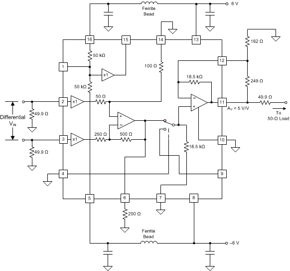
The most basic operation is to ground VREF (pin 14), and use the internal connection from the D2S to the OPS to provide a differential to single-ended, high-power driver. Figure 8-15 shows the characterization circuit used for the combined performance specifications.
 Figure 8-15 Differential to
Single-Ended, Gain of 5 V/V Configuration
Figure 8-15 Differential to
Single-Ended, Gain of 5 V/V ConfigurationThis configuration shows the test circuit used to generate Figure 6-1. Some of the key features in this basic configuration include:
- The power supplies are brought into the OPS first, then back to the input stage through a π-filter comprised of a ferrite bead and local decoupling capacitors on –VCC2 and +VCC2 (pins 5 and 16, respectively). See the Section 10 section for more information.
- The two logic lines are grounded. This logic configuration (with pin 7 grounded) selects the internal path from the D2S to OPS, and enables the OPS.
- The external I/O pins of the midscale buffer are left floating.
- The VREF pin is grounded, thus setting the D2S output common-mode voltage at VO1 (pin 6) to ground.
- The D2S external output is loaded with a 200 Ω resistor to ground. Lighter loading on the VO1 pin (versus the 100 Ω used to characterize the D2S only) results in increased frequency response peaking. Heavier loading degrades the D2S distortion performance.
- The external OPS input at VIN+ (pin 9) is left floating. However, VIN+ is internally tied to ground by the internal 18.5 kΩ resistor.
- The feedback resistor in the OPS is set to the parallel combination of the external 249 Ω resistor and the internal 18.5 kΩ resistor. This 245.7 Ω total RF with the 162 Ω RG resistor results in a gain of approximately 2.5 V/V (7.98 dB) in the OPS.
- The input D2S provides a gain of 2 V/V (6 dB), and along with the 2.5 V/V (7.98 dB) from the OPS, results in an overall gain of 5 V/V (13.98 dB) with > 600 MHz of SSBW (see Figure 6-1).