SBOS854F March 2018 – June 2024 TMP1075
PRODUCTION DATA
- 1
- 1 Features
- 2 Applications
- 3 Description
- 4 Device Comparison
- 5 Pin Configuration and Functions
-
6 Specifications
- 6.1 Absolute Maximum Ratings
- 6.2 ESD Ratings
- 6.3 Recommended Operating Conditions
- 6.4 Thermal Information
- 6.5 Electrical Characteristics:TMP1075
- 6.6 Electrical Characteristics: TMP1075N
- 6.7 Timing Requirements:TMP1075
- 6.8 Timing Requirements: TMP1075N
- 6.9 Switching Characteristics
- 6.10 Timing Diagrams
- 6.11 Typical Characteristics
-
7 Detailed Description
- 7.1 Overview
- 7.2 Functional Block Diagram
- 7.3
Feature Description
- 7.3.1 Digital Temperature Output
- 7.3.2
I2C and SMBus Serial Interface
- 7.3.2.1 Bus Overview
- 7.3.2.2 Serial Bus Address
- 7.3.2.3 Pointer Register
- 7.3.2.4 Writing and Reading to the TMP1075
- 7.3.2.5 Operation Mode
- 7.3.2.6 SMBus Alert Function
- 7.3.2.7 General Call- Reset Function
- 7.3.2.8 High-Speed Mode (HS)
- 7.3.2.9 Coexists in I3C Mixed Fast Mode
- 7.3.2.10 Time-Out Function
- 7.3.3 Timing Diagrams
- 7.3.4 Two-Wire Timing Diagrams
- 7.4 Device Functional Modes
- 7.5
Register Map
- 7.5.1
Register Descriptions
- 7.5.1.1 Temperature Register (address = 00h) [default reset = 0000h]
- 7.5.1.2 Configuration Register (address = 01h) [default reset = 00FFh (60A0h TMP1075N)]
- 7.5.1.3 Low Limit Register (address = 02h) [default reset = 4B00h]
- 7.5.1.4 High Limit Register (address = 03h) [default reset = 5000h]
- 7.5.1.5 Device ID Register (address = 0Fh) [default reset = 7500]
- 7.5.1
Register Descriptions
- 8 Application and Implementation
- 9 Device and Documentation Support
- 10Revision History
- 11Mechanical, Packaging, and Orderable Information
3 Description
The TMP1075 is the most accurate and lowest power replacement to the industry standard LM75 and TMP75 digital temperature sensors. Available in SOIC-8, VSSOP-8, WSON-8, and SOT563-6 packages, the TMP1075 offers pin-to-pin and software compatibility to quickly upgrade any existing xx75 design. The TMP1075 additional new packages are a 2.0mm × 2.0mm DFN and a 1.6mm × 1.6mm SOT563-6 reducing the printed circuit board (PCB) footprint by 82% and 89% compared to the SOIC package, respectively.
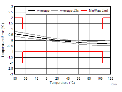
The TMP1075 has a ±1°C accuracy over a wide temperature range and offers an on-chip 12-bit analog-to-digital converter (ADC) providing a temperature resolution of 0.0625°C.
Compatible with two-wire SMBus and I2C interfaces, the TMP1075 support up to 32 device addresses and provides SMBus Reset and Alert function.
The TMP1075 D, DGK, and DSG packages are specified for operation over a temperature range of −55°C to 125°C and the TMP1075N DRL package is specified over the −40°C to 125°C temperature range.
The TMP1075 units are 100% tested on a production setup that is NIST traceable and verified with equipment that is calibrated to ISO/IEC 17025 accredited standards.
| PART NUMBER | PACKAGE(1) | PACKAGE SIZE(2) |
|---|---|---|
| TMP1075 | VSSOP (DGK, 8) | 3.00mm × 4.90mm |
| SOIC (D, 8) | 4.90mm × 6.00mm | |
| WSON (DSG, 8) | 2.00mm × 2.00mm | |
| SOT563 (DRL, 6)(3) | 1.60mm × 1.60mm |
 Simplified Schematic