SBOU240 October   2020 OPA455


  1.   Trademarks
  2. 1Overview
    1. 1.1 OPA455
    2. 1.2 OPA455EVM
    3. 1.3 Related Documentation
    4. 1.4 Evaluation Module Limitations and Cautions
      1. 1.4.1 High-Voltage Warning
      2. 1.4.2 Electrostatic Discharge Caution
  3. 2Getting Started
    1. 2.1 Power Supplies
    2. 2.2 Jumpers
    3. 2.3 Inputs
    4. 2.4 Outputs
    5. 2.5 Enable or Disable (E/D)
    6. 2.6 Status Flag
      1. 2.6.1 Circuit Protection
  4. 3Application Circuits
    1. 3.1 Improved Howland Current Pump
  5. 4Schematic, PCB Layout, and Bill of Materials
    1. 4.1 EVM Schematic
    2. 4.2 EVM Default Configuration
    3. 4.3 PCB Layout
    4. 4.4 Bill of Materials

PCB Layout

Figure 4-3 depicts the PCB layout.
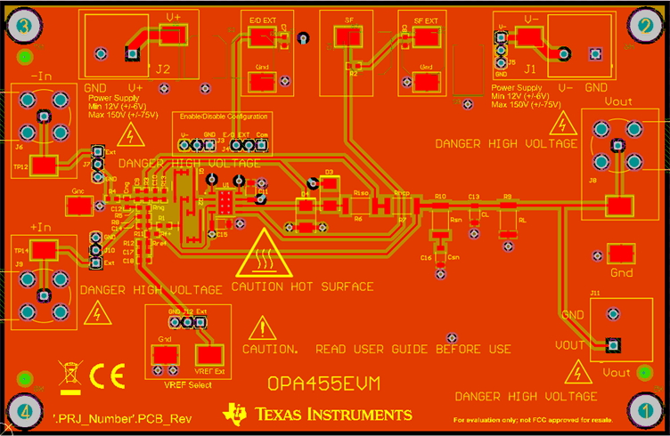
GUID-20200917-CA0I-NBDW-HXLP-PM3ZNXD9V09L-low.gifFigure 4-3 OPA455EVM PCB Layout
Note:

Board layout is not to scale. This figure is intended to show how the board is laid out, and is not intended to be used for manufacturing OPA455EVM PCBs.