SBOU297A April 2024 – July 2024
2.5 Setup
To test the parameters of the op amp, the test conditions must match those listed in the electrical characteristics table of the device. The following materials are required for all setup:
- AMP-PDK-EVM main board
- Package variant daughtercard
- Device-under-test (DUT)
- Triple power supply
Once the assembly instructions in Section 2.3 have been implemented, the following test setups can be referenced for common op amp parameters.
In addition to this section, step-by-step instructional videos are available on ti.com.
The equipment shown in these examples are for illustration purposes only.
Quiescent Current per Amplifier (IQ)
IQ is measured in series with the power supply source and the AMP-PDK-EVM.
Additional equipment needed for this test:
- Digital multimeter (DMM) or an ammeter
While referencing Section 2.3 to measure IQ,
- Install a daughtercard onto the Non-Inverting Gain = 1V/V (Buffer) preconfigured circuit.
- Connect the positive power supply in series with
a DMM:
- Connect V- and GND on AMP-PDK-EVM to the supplies on the triple power supply while matching the device's data sheet conditions. The current limit of the power supply must be set to at least 10 times the IQ (considering all channels).
- Connect V+ on AMP-PDK-EVM to the appropriate port on the DMM.
- Connect the other port from the DMM to the positive power supply on the triple power supply. Limit the output current to at least 10 times the IQ (considering all channels).
- Depending on how many channels the op amp has, the daughtercard has all possible pins mapped out. All INx+ pins on the sub-circuit must be connected to GND.
- Configure the DMM to measure DC current.
- Turn on the power supply output.
- On the DMM, divide the observed current by the number of channels in the op amp.
With all other data sheet conditions matched, this test setup helps verify the quiescent current in the data sheet with the one calculated. (1)
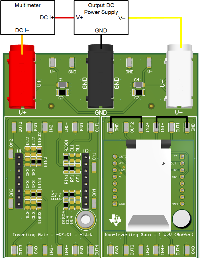 Figure 2-10 Iq Measurement Example Setup for a
Dual Channel Device
Figure 2-10 Iq Measurement Example Setup for a
Dual Channel DeviceContinuity
Most op amp pins have ESD protection diodes to either power supply rail (V+ or V-). To check for the presence and operation of these diodes, follow this procedure.
Additional equipment needed for this test:
- Digital multimeter (DMM) or an ammeter
While referencing Section 2.3 to measure continuity,
- Install a daughtercard onto the pin-to-pin circuit.
- Connect the power supply's positive supply to the appropriate port of the DMM. The current limit of the power supply must be set to 9mA.
- The ground from the power supply and the other port on the DMM are the two points of continuity, due to the nature of ESD diodes, one must be referenced to a power supply V+_p2p or V-_p2p; the other is the pin-under-test.
- Turn on the power supply output.
- Manually increase the power supply output voltage in small increments, recording the current between increments, until the measured current reaches a maximum of 9mA. Do not exceed 2-3V in either direction.
- Depending on how many channels the op amp has, the daughtercard has all possible pins mapped out. All INx+ , INx-, and OUTx pins can be tested against V+_p2p or V-_p2p.
Alternatively, this test can be automated with a source meter.
This test setup helps verify the presence and operation of ESD diodes.
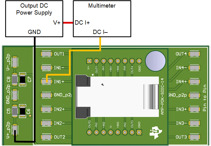 Figure 2-11 Continuity Measurement Example Setup
for a Quad Channel Device
Figure 2-11 Continuity Measurement Example Setup
for a Quad Channel DeviceInput Offset Voltage (VOS)
VOS is an error source at the input stage of the op amp, quantified as the differential input voltage needed to force the op amp's output to 0V.
Additional equipment needed for this test:
- Digital multimeter (DMM) or a voltmeter
While referencing Section 2.3 to measure VOS,
- Install a daughtercard onto the Non-Inverting Gain = 1001V/V or Non-Inverting Gain = 101V/V preconfigured circuit depending on the typical or expected offset voltage of the device. In general, use the Non-Inverting Gain = 1001V/V for precision op amps and Non-Inverting Gain = 101V/V for general purpose op amps.
- Connect the triple power supply to the V+, GND, and V- of AMP-PDK-EVM while matching the data sheet conditions of the device. The current limit of the power supply can be set to the ISC + IQ of the device (considering all channels).
- Depending on how many channels the op amp has, the daughtercard has all possible pins mapped out. All INx+ pins on the sub-circuit needs to be connected to GND.
- Connect one port of the DMM to OUTx and the other to GND.
- Configure the DMM to measure DC voltage.
- Turn on the power supply output.
- Divide the voltage measurement of DMM by the gain of the preconfigured circuit.
With all other data sheet conditions matched, this test setup helps verify the input offset voltage in the data sheet with the one calculated.
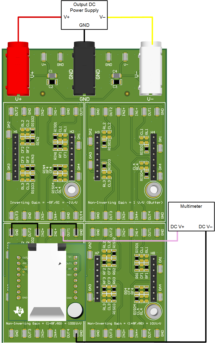 Figure 2-12 Vos Measurement Example Setup for a
Dual Channel Device
Figure 2-12 Vos Measurement Example Setup for a
Dual Channel DeviceVoltage Output Swing from Supply Voltages (VOL/VOH)
VOH and VOL are the voltage limit of the output of the op amp as the output approaches the V+ and V- of the device.
Additional equipment needed for this test:
- Digital multimeter (DMM) or a voltmeter
While referencing Section 2.3 to measure VOH and VOL
- Install a daughtercard onto the Non-Inverting Gain = 1V/V (Buffer) preconfigured circuit. For non-rail-to-rail input op amps, the amplifier needs to be placed in a gain to try to force the output to either rail.
- Connect the triple power supply to the V+, GND, and V- of AMP-PDK-EVM while matching the device's data sheet conditions. The current limit of the power supply needs to be set to the ISC + IQ of the device (considering all channels).
- Connect the single power supply between INx+ pin and GND. Set the single supply voltage to the V+ value of the op amp. The current limit of the power supply must be set to 9mA.
- Connect one port of the DMM to OUTx and the other to GND.
- Depending on how many channels the op amp has, the daughtercard has all possible pins mapped out. All other INx+ pins on the sub-circuit must be connected to GNDquie.
- Configure DMM to measure DC voltage.
- Turn on the triple power supply first; subsequently, turn on the single power supply.
- The VOH is the difference between V+ and the voltage measured on the DMM.
- Swap the single supply connections listed in Step #3. The positive supply must be connected to GND and ground from the supply must be connected to +INx pin.
- The VOL is the difference between V+ and absolute value of voltage measured on the DMM.
With all other data sheet conditions matched, this test setup helps verify the voltage output swing from rail in the data sheet with the calculated.
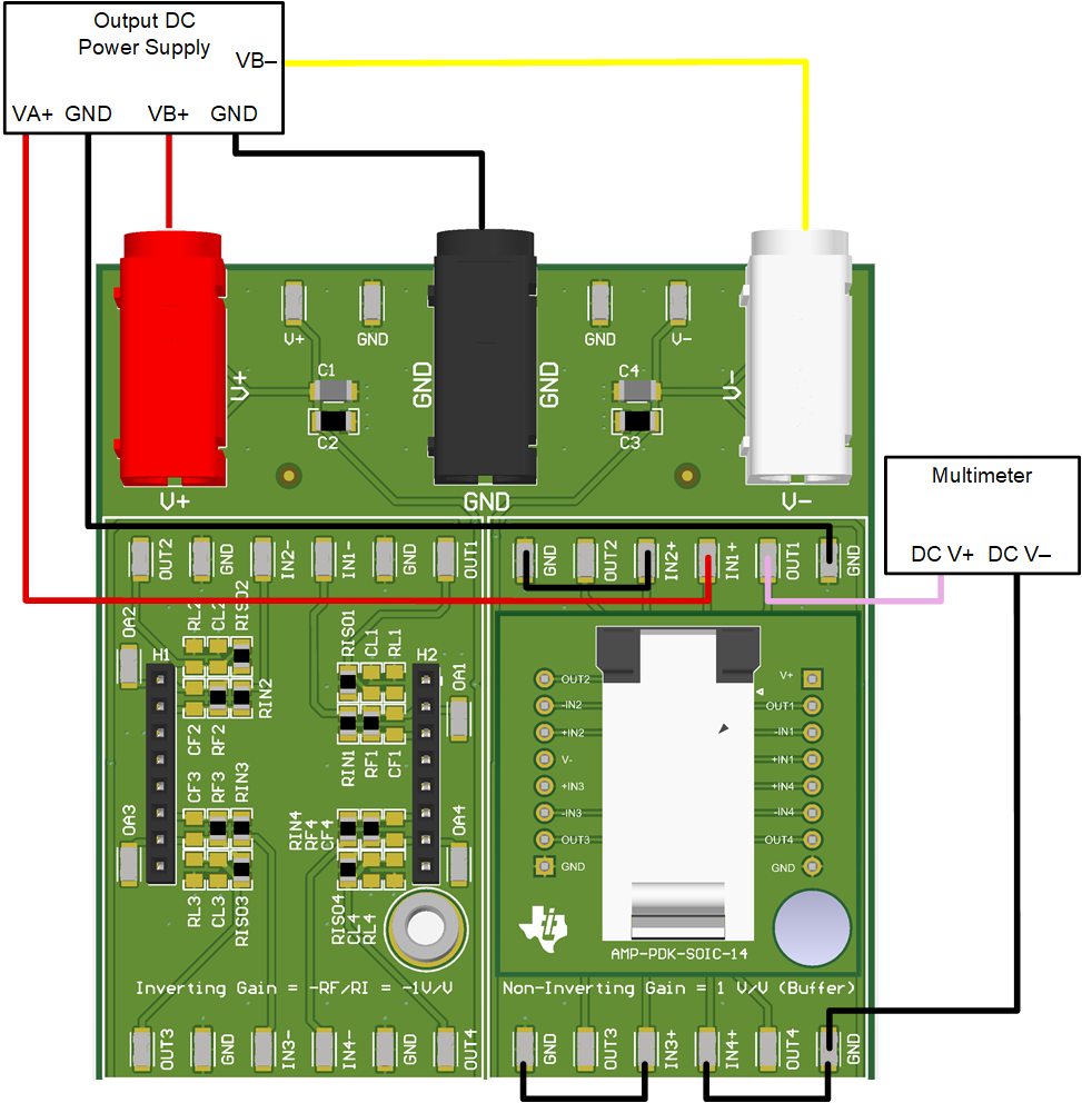 Figure 2-13 VOH Measurement Example for a Quad
Channel Device
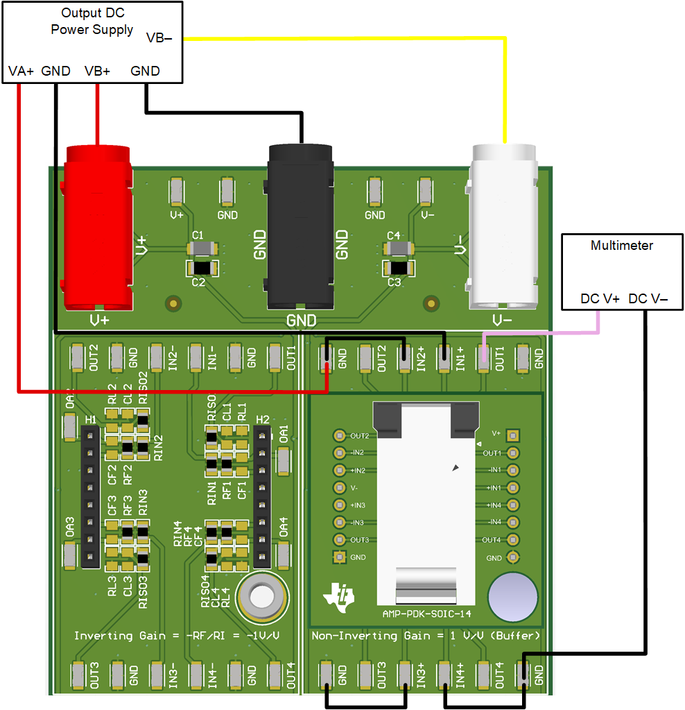 Figure 2-14 VOL Measurement Example for a Quad
Channel Device
Figure 2-14 VOL Measurement Example for a Quad
Channel DeviceGain Bandwidth Product (GBWP)
Additional equipment needed for this test:
- Digital multimeter (DMM) or a voltmeter
- Waveform function generator
While referencing Section 2.3 to measure GBW,
- Install a daughtercard onto the Non-Inverting Gain = 101V/V preconfigured circuit.
- Connect the triple power supply to the V+, GND, and V- of AMP-PDK-EVM while matching the device's data sheet conditions. The current limit of the power supply must be set to the ISC + IQ of the device (considering all channels).
- Connect the output of the frequency generator to the INx+ pin and reference to GND.
- Depending on how many channels the op amp has, the daughtercard has all possible pins mapped out. All other INx+ pins on the sub-circuit must be connected to GND.
- Connect one DMM port to OUTx and the other to GND.
- Turn on the power supply output.
- Configure the waveform generator to output a small signal (20mVpp, 100Hz, 0 offset voltage).
- Turn on the waveform function generator.
- Configure DMM to measure AC voltage. Record the DMM voltage.
- Increase the frequency on the waveform generator until the DMM reads 70.7% of the original DMM voltage. Record the frequency of the waveform generator.
- Divide the frequency by the gain of the preconfigured circuit.
With all other data sheet conditions matched, this test setup helps verify the gain bandwidth product in the data sheet with the calculated.
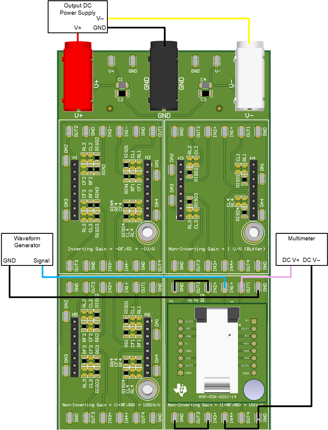 Figure 2-15 BW Measurement Example for Quad
Channel Device
Figure 2-15 BW Measurement Example for Quad
Channel DeviceSlew Rate (SR)
SR is the maximum rate of change of an op amp's output voltage in volts per microsecond.
Additional equipment needed for this test:
- Oscilloscope
- Waveform function generator
While referencing Section 2.3 to measure SR,
- Install a daughtercard onto the Non-Inverting Gain = 1V/V (Buffer) preconfigured circuit.
- Connect the triple power supply to the V+, GND, and V- of AMP-PDK-EVM while matching the device's data sheet conditions. The current limit of the power supply must be set to the ISC + IQ of the device (considering all channels).
- Connect the waveform generator to the INx+ pin with a reference to GND. The input signal must be step function the size of the input voltage common mode listed in the data sheet.
- Depending on how many channels the op amp has, the daughtercard has all possible pins mapped out. All other INx+ pins on the sub-circuit must be connected to GND.
- Connect an oscilloscope probe to the OUTx with a probe referenced to GND.
- Turn on the power supply output.
- Turn on the waveform function generator.
- Configure the oscilloscope to measure approximately 10% and 90% of the output waveform, note the time differential. Slew rate is the rate of change in volts per microsecond.
With all other data sheet conditions matched, this test setup helps verify the slew rate in the data sheet with the one calculated.
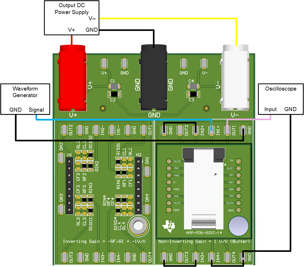 Figure 2-16 SR Measurement Example for a Single
Channel Device
Figure 2-16 SR Measurement Example for a Single
Channel DeviceComparators Setup
The AMP-PDK-EVM kit has the capability of testing basic functionality of comparators using the pin-to-pin circuit. Do not test a comparator device with any of the other gain configurations as this can result in measurement errors. Positive feedback or hysteresis setup is not available with the board.
The backside of the pin-to-pin board contains an option to populate pull-up resistors Rupx on the output of the comparator, as shown in Figure 3-17. By default, Rupx are unpopulated.
Rupx is required to populate for any comparator that has an open-drain/open-collector output type. Without the pull-up resistor, the output of the comparator can float to an unknown state. This resistor does not need to be populated when using push-pull devices. The output type of the comparator can be verified in the product page and data sheet.
For more information on comparators, please reference TI Precision Labs.
 Figure 2-17 Pin-to-Pin Circuit (Back View)
 Figure 2-18 Pin-to-pin Schematic with Pull-Up
Resistor Option
Figure 2-18 Pin-to-pin Schematic with Pull-Up
Resistor OptionAdvanced Test Setup
The above test setups are solderless preconfigured op amp designs with the options of a gain of 1, 101, 1001, and -1. The board can also be re-purposed in different gain ratios by changing the passive components. In addition to the existing populated passives, there is compensation circuitry options included to limit noise (CF) and help improve stability (RISO) as seen in Schematics. The OAx test point is given to help verify amplifier stability. For more resources on op amp noise and stability, please reference TI Precision Labs.