SBOU314 June 2024 TRF1305B2
2.1 General Usage Information
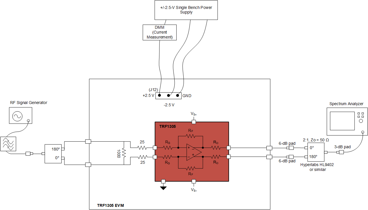
 Figure 2-1 Single Tone Setup for Gain and Output P1dB
This section provides general usage information for the EVM. See Figure 3-1 for a general single tone setup diagram as a reference point for the following instructions (some components, such as supply bypass capacitors, are omitted for clarity):
- Recommended power up sequence:
- Split-supply operation:
- To operate as split supply, apply the positive supply voltage to VS+, negative supply voltage to VS– , and the ground reference from supply to GND (J12). The supply voltages do not need to be symmetrical, provided that the total supply voltage is 5V, any combination of positive and negative supply voltages is acceptable. This feature is often used when the output common mode voltage must be set to a particular value. For best performance, the power supply voltages must be symmetrical around the desired output common-mode voltage.
- Set the current limit of the DC output power supply at 250mA.
- Making sure the supply is turned off, connect the power supply cables to the J12 connector of the EVM.
- Now turn on the DC power supply of VS+ = 2.5V and VS- = -2.5V. The supply current (IQ) drawn from the power supply is approximately 180mA.
- If the supply current is low, then verify that the device is not disabled by the PD pin (J17, J9).
- Single-supply operation:
- To operate as single supply, connect jumper VS– to GND (J11), and apply the positive supply voltage to VS+ (J12). Inputs and outputs must be biased as in the TRF1305 data sheet specifications for proper operation.
- Split-supply operation:
- Power-down option:
- Connect +1.8 V (logic-1) on PD pin to power-down the chip (J9, J17). Ground the PD pin to enable the chip.
- CM (output common mode voltage) input:
- The TRF1305 device has an output common-mode control pin that sets the output common mode voltage. The output common-mode voltage at the output pins, OUTPx and OUTMx, defaults to the LDO output voltage of VS– + 2.5V when VOCM pin is floated.
- If a different output common-mode voltage is specified, then the J23 jumper can be used to connect an external low-impedance voltage source. See the TRF1305 data sheet for performance curves that show how performance is impacted by an output common mode voltage that is not at the mid-supply voltage.
- Single tone measurement setup recommendation:
- Single ended signal from RF signal generator is converted to a differential signal using an external passive balun as shown in Figure 3-1. Differential signal is fed to input SMA connectors, J1, J2.
When measuring single tone distortion, use an RF band pass filter as shown in Figure 3-1. - The RF signal generator used must support up to 10GHz signal frequency for testing out the EVM.
- The device input is 50Ω in the pass-band.
To minimize signal reflections due to impedance mismatch, TI recommends using an attenuator pad of approximately 3dB to 6dB between the source and J4 SMA input. - The EVM outputs are fully differential (or 180° out-of-phase) at J5 and J6 SMA connectors.
The device has low output impedance at dc and low frequencies. - When connecting to a spectrum analyzer, the differential signal out of the EVM must be converted to a single-ended signal using an external passive balun as shown in Figure 3-1.
Usage of an attenuator pad of approximately 3dB to 6dB is recommended at the three terminals of the passive balun to minimize reflections. - Lastly, TI recommends to properly characterize and account for the insertion loss of RF coaxial (coax) cables, attenuator pads, and passive baluns to measure accurate gain and power levels for the device.
- Single ended signal from RF signal generator is converted to a differential signal using an external passive balun as shown in Figure 3-1. Differential signal is fed to input SMA connectors, J1, J2.