SBOU315 March 2024 PGA849
3.2 PCB Layout
The PGA849EVM is a four-layer PCB design. Figure 4-2 to Figure 4-6 show the PCB layer illustrations. The top layer consists of all signal path traces, and is poured with a solid ground plane. A symmetrical board layout is used at the differential inputs to keep good performance matching and improve common-mode noise rejection. Route traces as symmetrically as possible for both positive and negative pathways. The optional differential input low-pass filter capacitor is placed in very close proximity to the PGA inputs to reduce extrinsic noise. Capacitor C17 is placed in close proximity to REF pin to avoid injecting noise. Decoupling capacitors C2, C15, C3 and C16 are positioned on the top layer as close as possible to the power-supply pins of the device. The second internal layer is a dedicated solid GND plane. The voltage source applied to the reference pin must have a low output impedance. Any resistance at the REF pin is in series with an internal 5kΩ resistor that creates an imbalance in the four resistors of the internal difference amplifier. Optional OPA192 buffer (U2) is placed in close proximity to the REF pin to minimize series resistance in the REF pin. Independent vias are placed at the ground connection of every component to provide a low-impedance path to ground. The third internal layer and bottom layer route the input stage power supplies and the output-stage supply connections.
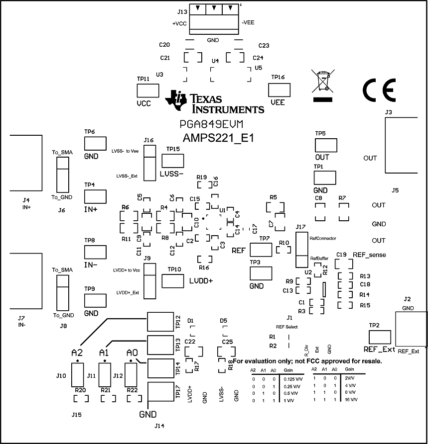 Figure 3-2 Top Overlay PCB
Layout
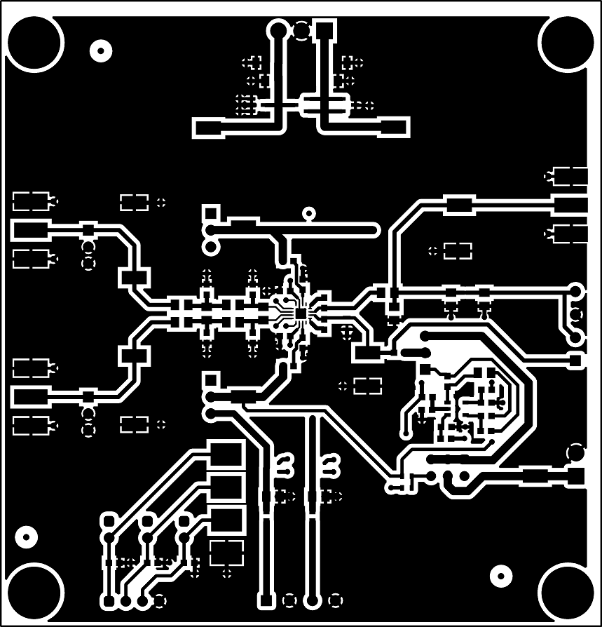 Figure 3-3 Top Layer PCB
Layout
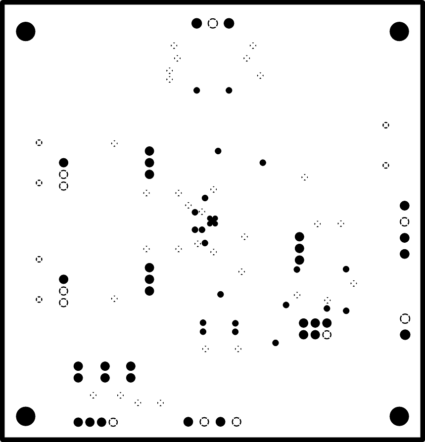 Figure 3-4 Ground Layer PCB
Layout
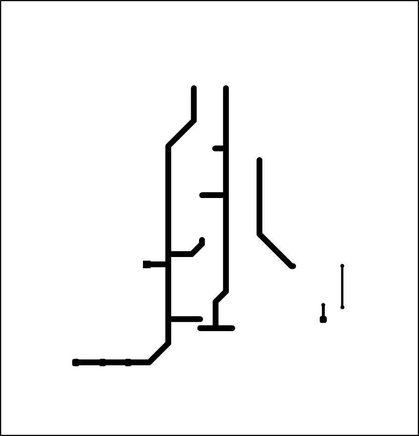 Figure 3-5 Power Layer PCB
Layout
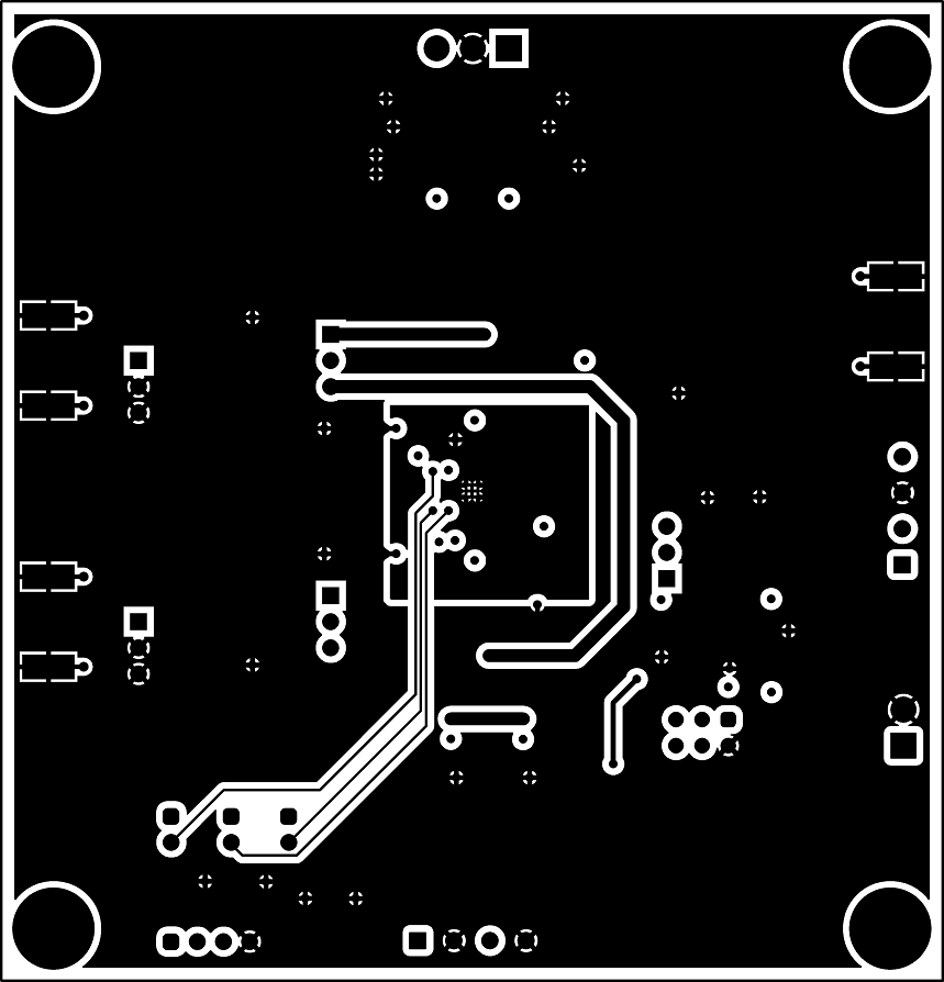 Figure 3-6 Bottom Layer PCB
Layout