SBVS066S December 2005 – November 2024 TPS74401
PRODUCTION DATA
- 1
- 1 Features
- 2 Applications
- 3 Description
- 4 Pin Configuration and Functions
- 5 Specifications
- 6 Detailed Description
- 7 Application and Implementation
- 8 Device and Documentation Support
- 9 Revision History
- 10Mechanical, Packaging, and Orderable Information
7.4.1.1 Power Dissipation
Knowing the device power dissipation and proper sizing of the thermal plane that is connected to the tab or pad is critical to avoiding thermal shutdown and verifying reliable operation.
Power dissipation of the device depends on input voltage and load conditions, and can be calculated using Equation 6:
Power dissipation can be minimized and greater efficiency can be achieved by using the lowest possible input voltage necessary to achieve the required output voltage regulation.
On the VQFN (RGW, RGR) packages, the primary conduction path for heat is through the exposed pad to the PCB. The pad can be connected to ground or left floating; however, the pad must attach to an appropriate amount of copper PCB area to verify that the device does not overheat. On the DDPAK (KTW) package, the primary conduction path for heat is through the tab to the PCB. Connect that tab to ground. The maximum junction-to-ambient thermal resistance depends on the maximum ambient temperature, maximum device junction temperature, and power dissipation of the device and can be estimated using Equation 7:
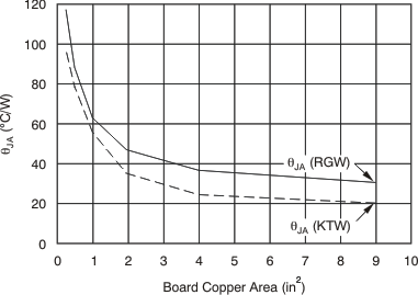
Knowing the maximum RθJA, the minimum amount of PCB copper area needed for appropriate heat sinking is estimated using Figure 7-14.

Figure 7-14 shows the variation of θJA as a function of ground plane copper area in the board. Figure 7-14 is intended only as a guideline to demonstrate the affects of heat spreading in the ground plane; do not use Figure 7-14 to estimate actual thermal performance in real application environments.
When the device is mounted on an application PCB, TI strongly recommends using ΨJT and ΨJB, as explained in the Thermal Information table.