SBVS398A December   2021  – September 2022 TPS7A21

PRODUCTION DATA  

  1. Features
  2. Applications
  3. Description
  4. Revision History
  5. Pin Configuration and Functions
  6. Specifications
    1. 6.1 Absolute Maximum Ratings
    2. 6.2 ESD Ratings
    3. 6.3 Recommended Operating Conditions
    4. 6.4 Thermal Information
    5. 6.5 Electrical Characteristics
    6. 6.6 Typical Characteristics
  7. Detailed Description
    1. 7.1 Overview
    2. 7.2 Functional Block Diagram
    3. 7.3 Feature Description
      1. 7.3.1 Smart Enable (EN)
      2. 7.3.2 Low Output Noise
      3. 7.3.3 Active Discharge
      4. 7.3.4 Dropout Voltage
      5. 7.3.5 Foldback Current Limit
      6. 7.3.6 Undervoltage Lockout
      7. 7.3.7 Thermal Overload Protection (TSD)
    4. 7.4 Device Functional Modes
      1. 7.4.1 Device Functional Mode Comparison
      2. 7.4.2 Normal Operation
      3. 7.4.3 Dropout Operation
      4. 7.4.4 Disabled
  8. Applications and Implementation
    1. 8.1 Application Information
      1. 8.1.1 Recommended Capacitor Types
      2. 8.1.2 Input and Output Capacitor Requirements
      3. 8.1.3 Load Transient Response
      4. 8.1.4 Undervoltage Lockout (UVLO) Operation
      5. 8.1.5 Power Dissipation (PD)
      6. 8.1.6 Estimating Junction Temperature
      7. 8.1.7 Recommended Area For Continuous Operation
    2. 8.2 Typical Application
      1. 8.2.1 Design Requirements
      2. 8.2.2 Detailed Design Procedure
        1. 8.2.2.1 Power Dissipation and Device Operation
      3. 8.2.3 Application Curves
    3. 8.3 Power Supply Recommendations
    4. 8.4 Layout
      1. 8.4.1 Layout Guidelines
        1. 8.4.1.1 DSBGA Mounting
        2. 8.4.1.2 DSBGA Light Sensitivity
      2. 8.4.2 Layout Example
  9. Device and Documentation Support
    1. 9.1 Device Support
      1. 9.1.1 Device Nomenclature
    2. 9.2 Documentation Support
      1. 9.2.1 Related Documentation
    3. 9.3 Receiving Notification of Documentation Updates
    4. 9.4 Support Resources
    5. 9.5 Trademarks
    6. 9.6 Electrostatic Discharge Caution
    7. 9.7 Glossary
  10. 10Mechanical, Packaging, and Orderable Information
    1. 10.1 Mechanical Data

Application Curves

GUID-20211209-SS0I-TMLB-B2FB-Q6CG4XVBGBRL-low.jpg
VIN = 0 V to 4.3 V, slew rate = 1 V/μs, IOUT = 1 mA
Figure 8-5 Start-Up With VEN After VIN
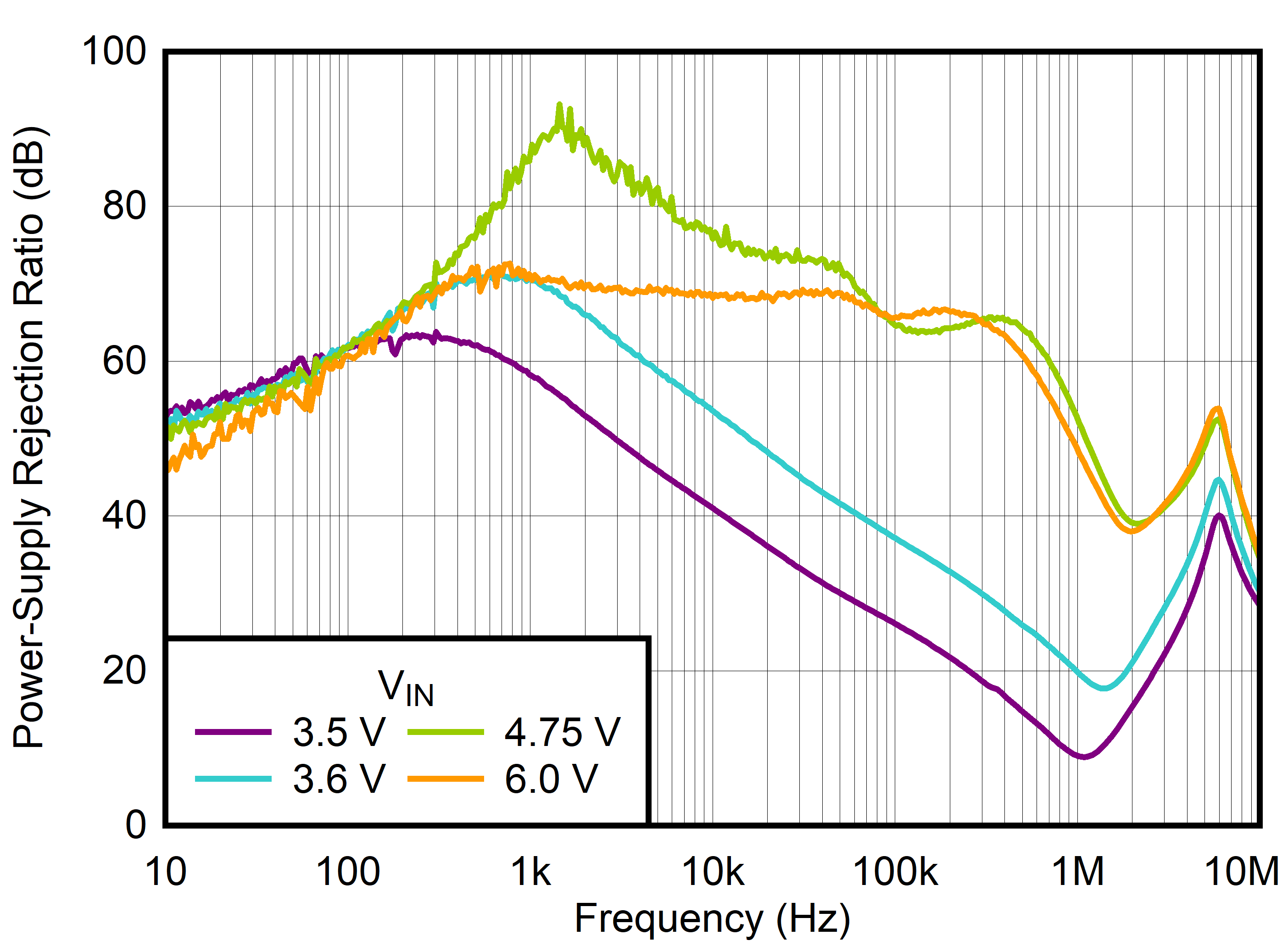
GUID-20211122-SS0I-M811-S9DD-MKC4G8ZPPCX8-low.png
VEN = VIN, IOUT = 500 mA
Figure 8-6 PSRR vs Frequency and VIN